LabAdviser/Technology Research/Fabrication of Hyperbolic Metamaterials using Atomic Layer Deposition/AZO pillars
Feedback to this page: click here
This page is written by Evgeniy Shkondin @DTU Nanolab if nothing else is stated.
All images and photos on this page belongs to DTU Nanolab and DTU Electro (previous DTU Fotonik).
The fabrication and characterization described below were conducted in 2013-2016 by Evgeniy Shkondin, DTU Nanolab.
Procces flow description
Double side polished (DSP), 150 mm (100) Si wafers were selected for device fabrication. They were RCA cleaned and later oxidized in a conventional quartz tube (furnace from Tempress) using a dry oxidation process based on O2 at 1100 °C, resulting in a 200 nm SiO2 layer on Si. Next, a 2 μm amorphous Si layer was deposited on the SiO2 surface using a conventional low-pressure chemical vapor deposition (LPCVD) process (furnace from Tempress) based on SiH4 at 560 °C. This procedure enables the preparation of home-made silicon-on-insulator (SOI) substrates.
The main steps in the fabrication of pillars and tubes are shown in Fig 1. Initially, silicon holes were etched in SOI wafers by deep-UV lithography and DRIE (Fig. 1(a)-1(c)). The holes were arranged in a square lattice with the pitch of 400 nm. The template was then filled with an ALD D25 AZO coating (Fig. 1(d)) at 250 °C. The thickness of the deposited AZO depends on the desired output. An entire filling would result in the formation of pillars, while partial deposition leads to fabrication of hollow tubes. After removal of the top parts by Ar+ ion sputtering (Fig. 1(e)), the silicon core between the ALD coated holes was etched away during the last step. Figure 1(f) represents the final structures. Fabrication output is shown in Fig. 2. Each process step was carefully analyzed using cross-sectional SEM imaging (see Figs. 3 and 4 for pillars and tubes fabrication, respectively).
-
 Figure 1. Schematics of the fabrication flow. a) Home-made SOI substrates. b) Deep-UV lithography. Resist spin coating, baking, exposure and developing. c) DRIE etching, fabrication of initial Si template. d) ALD deposition of D25 AZO at 250 °C. Partial deposition will lead to fabrication of tubes, while complete filling will create full pillars. e) Removal of the top AZO layer by Ar+ sputtering. f) Silicon host removal using conventional RIE process.
 -
 Figure 2. SEM images, bird-eye-view. a) AZO pillars, and b) AZO tubes.


-
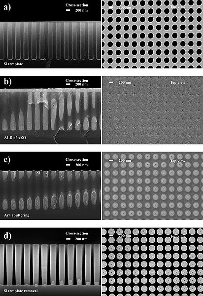 Figure 3. SEM verification for each fabrication step of pillars production. Substrate is normal Si-wafer. Left side shows cross-sectional images and right side of the Figure shows the top view of the structures.
 -
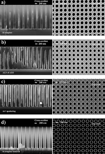 Figure 4. SEM verfication for each fabrication step of tube production. Substrate is silicon-on-isolator (SOI). Left side shows cross-sectional images and right side of the Figure shows the top view of the structures.


Process flow
Description of steps for fabrication of AZO nanopillars and tubes.
| Step | Description | LabAdviser link | Image showing the step | |
|---|---|---|---|---|
| 1.1 | RCA.(Optional step. Needs only if SOI substrates requires) | To ensure a clean surface before furnace processing, the wafers needs to be RCA cleaned. |  | |
| 1.2 | Thermal oxidation of Si.(Optional step. Needs only if SOI substrates requires) | Creating 200 nm thin SiO2 layer using Dry Oxidation process in a C1 Furnace Anneal-oxide equipment. | C1 Furnace Anneal-oxide. |  |
| 1.3 | LPCVD deposition of Si. (Optional step. Needs only if SOI substrates requires) | LPCVD of amorphous silicon using AMORPOLY recipe in 6" Furnace LPCVD PolySilicon. | 6" Furnace LPCVD PolySilicon. |  |
| 1.4 | DUV Resist patterning. | DUV | DUV Stepper Lithography. |  |
| 1.5 | Deep reactive ion etching (DRIE). | DRIE; Recipe: PolySOI10 Recipe needs to be tuned. Adjusted parameters: temperature, etching and passivation times. | DRIE Pegasus. |  |
| 1.6 | Plasma surface treatment. | To ensure that remainings of DUV resist are gone, samples are treated by O2/N2 plasma. (Optional step) | ||
| 1.7 | Scanning Electron Microscopy inspection. | By cleaving the sample it is possible to inspect DRIE etched Si holes in cross-sectional mode. | See Figures 3a and 4a above. | |
| 1.8 | Atomic Layer Deposition of Al-doped ZnO (AZO). | Deposition carried at 250oC. For compleate pillars the thickness needs to above 100 nm. For AZO tubes only 20 nm (partial deposition) requires. | Equipment used: ALD Picosun R200. Standard recipe used: AZO 25T. |  |
| 1.9 | Scanning Electron Microscopy inspection. | By cleaving the sample it is possible to inspect ALD coatings deposited in Si holes in cross-sectional mode. | See figures 3b and 4b above. | |
| 1.10 | Ion Beam Etching (IBE). | Opening of deposited AZO top layer using recipe "Ti acceptance" there the stage was placed to 0o degree. The back side of the wafer also needs to be exposed to etching. | IBE/IBSD Ionfab 300 |  |
| 1.11 | Scanning Electron Microscopy inspection. | By cleaving the sample it is possible to inspect IBE etching results in cross-sectional mode. | See Figures 3c and 4c above. | |
| 1.12 | Selective etch of Si between ALD AZO coatings. | Si etching proceeds using reactive ion etching with isotropic process based on SF6 process gas. | Equipment used: RIE2. |  |
| 1.13 | Scanning Electron Microscopy inspection of fabricated structures. | Proof of final result. | See Figures 2, 3d and 4d above. | |