Specific Process Knowledge/Thin film deposition/Electroplating-Ni: Difference between revisions
| Line 46: | Line 46: | ||
|style="background:WhiteSmoke; color:black"|<b>Value</b> | |style="background:WhiteSmoke; color:black"|<b>Value</b> | ||
|- | |- | ||
!style="background:silver; color:black" align="center" valign="center" rowspan=" | !style="background:silver; color:black" align="center" valign="center" rowspan="1"|Sample dimensions | ||
|style="background:LightGrey; color:black"|Diameter | |style="background:LightGrey; color:black"|Diameter | ||
|style="background:WhiteSmoke; color:black"| | |style="background:WhiteSmoke; color:black"| | ||
100 or 150 mm 4" or 6") | |||
|- | |- | ||
!style="background:silver; color:black" align="center" valign="center" rowspan="2"|Process parameters | !style="background:silver; color:black" align="center" valign="center" rowspan="2"|Process parameters | ||
|style="background:LightGrey; color:black"|Temperature | |style="background:LightGrey; color:black"|Temperature | ||
|style="background:WhiteSmoke; color:black"| | |style="background:WhiteSmoke; color:black"| | ||
30*C | |||
|- | |- | ||
|style="background:LightGrey; color:black"|pH | |style="background:LightGrey; color:black"|pH | ||
|style="background:WhiteSmoke; color:black"| | |style="background:WhiteSmoke; color:black"| | ||
acidic | |||
|- | |- | ||
!style="background:silver; color:black" align="center" valign="center" rowspan="3"|Sample requirements | !style="background:silver; color:black" align="center" valign="center" rowspan="3"|Sample requirements | ||
|style="background:LightGrey; color:black"|Seed metal | |style="background:LightGrey; color:black"|Seed metal | ||
|style="background:WhiteSmoke; color:black"| | |style="background:WhiteSmoke; color:black"| | ||
NiV. | 100 nm of either NiV, Ti/Au or Cr/Au recommended. Most commonly seed metals are sputtered using the [[Specific Process Knowledge/Thin film deposition/Lesker|Sputter-System(Lesker)]]. | ||
|- | |- | ||
| style="background:LightGrey; color:black"|Allowed materials | | style="background:LightGrey; color:black"|Allowed materials | ||
|style="background:WhiteSmoke; color:black"| | |style="background:WhiteSmoke; color:black"| | ||
Ask | Ask Customer Support for details | ||
|- | |- | ||
| style="background:LightGrey; color:black"|Forbidden materials | | style="background:LightGrey; color:black"|Forbidden materials | ||
|style="background:WhiteSmoke; color:black"| | |style="background:WhiteSmoke; color:black"| | ||
Ask | Ask Customer Support for details | ||
|} | |||
<br clear="all" /> | <br clear="all" /> | ||
Revision as of 14:27, 26 June 2015
Feedback to this page: click here
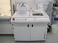
Technotrans microform.200

The Technotrans microform.200 (Electroplating-Ni in LabManager) is a machine capable of depositing nickel electrochemically. This is done by lowering the sample into an electrolyte containing nickel ions and then apply a voltage across the sample and the anode. The anode is a basket filled with nickel pellets. The cathode is the sample to be coated with nickel.
At the anode metallic nickel is oxidized to nickel ions:
Ni (s) ⇒ Ni2+ (aq) + 2 e-
At the cathode (the sample surface), nickel ions from solution are reduced to metallic nickel:
Ni2+ (aq) + 2 e- ⇒ Ni (s)
The minimal charge accepted by the software on the machine is 0.1 Ah (Ampere-hours). This corresponds to roughly 2 µm of nickel on a four inch wafer. You can abort a program prematurely to achieve even lower thicknesses, but this requires manual control of the machine.
The maximum allowed thickness is ~1,4 mm (1400 µm), since a higher thickness will make the release of the sample difficult and likely damage the sample holder. This corresponds to a charge of 53-54 Ah on a four inch wafer.
The plating bath is an aqueous solution of nickel sulfamate, boric acid and sulfamic acid. The bath is moderately acidic (pH = 3,5 - 3,8) and the temperature of the bath is around 52°C. The sample will spin at 60 RPM during deposition.
Uniformity across a 4" wafer is around 5% for the standard processes (the edge being slightly thicker than the center of the sample). Running at high current densities will deposit a nickel layer that is quite soft. Decreasing current density will increase tensile strength of the deposited nickel.
The user manual(s), quality control procedure(s) and results, user APV(s), technical information and contact information can be found in LabManager:
Electroplating-Ni Info on LabManager
Process information
| Parameter | Value | |
|---|---|---|
| Sample dimensions | Diameter |
100 or 150 mm 4" or 6") |
| Process parameters | Temperature |
30*C |
| pH |
acidic | |
| Sample requirements | Seed metal |
100 nm of either NiV, Ti/Au or Cr/Au recommended. Most commonly seed metals are sputtered using the Sputter-System(Lesker). |
| Allowed materials |
Ask Customer Support for details | |
| Forbidden materials |
Ask Customer Support for details | |
