|
|
| Line 259: |
Line 259: |
| ==Overview of sample processing 3== | | ==Overview of sample processing 3== |
| {| class="wikitable collapsible" border="1" cellspacing="1" cellpadding="2" align="left" | | {| class="wikitable collapsible" border="1" cellspacing="1" cellpadding="2" align="left" |
| ! Clean the sample |} | | ! Clean the sample |
| | |} |
| {| class="wikitable collapsible" border="1" cellspacing="1" cellpadding="2" align="left" | | {| class="wikitable collapsible" border="1" cellspacing="1" cellpadding="2" align="left" |
| ! Drying Samples |} | | ! Drying Samples |
| | |} |
|
| |
|
| {| class="wikitable collapsible collapsed" border="1" cellspacing="1" cellpadding="2" align="left" | | {| class="wikitable collapsible collapsed" border="1" cellspacing="1" cellpadding="2" align="left" |
Revision as of 12:27, 12 June 2014
2nd Level - Process Topic
Feedback to this page: click here
Choose the process topic you are interested in
The section below here is under construction 
Overview of sample processing
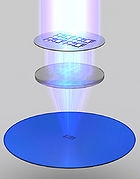
| Make a layer on the sample or Film Formation File:Making a layer 1.jpg
|
| Thermal Oxide growth
|
|
| Physical Vapour Deposition
|
|
|
|
Sputter deposition
|
|
|
Thermal deposition
|
|
|
E-beam evaporation
|
| CVD
|
|
|
|
LPCVD
|
|
|
PECVD
|
| Coating
|
|
|
|
Spin coating
|
|
|
Spray coating
|
| Electroplating
|
|
| Epitaxial growth
|
|
Make a mask on the sample 
|
| Lithography
|
| Imprinting
|
| Transfer pattern into the sample
|
| Wet etch
|
| Dry etch
|
| Lift-off
|
| Direct structure definition
|
| Imprinting
|
| LASER machining
|
| Lithographic definition
|
| Polymer Injection molding
|
| Back end of the sample
|
| Chip/die mounting
|
| Wire bonding
|
| Dicing
|
Overview of sample processing 2
|
|
|
| File:Making a layer 1.jpgFilm Formation
|
| Thermal Oxide growth
|
|
| Thin Film deposition
|
|
|
|
Sputter deposition
|
|
|
Thermal deposition
|
|
|
E-beam evaporation
|
| CVD
|
|
|
|
LPCVD
|
|
|
PECVD
|
| Coating
|
|
|
|
Spin coating
|
|
|
Spray coating
|
| Electroplating
|
|
| Epitaxial growth
|
|
|
|
 Make a mask on the sample Make a mask on the sample
|
| Lithography
|
| Imprinting
|
|
| Transfer pattern into the sample
|
| Wet etch
|
| Dry etch
|
| Lift-off
|
|
| Direct structure definition
|
| Imprinting
|
| LASER machining
|
| Lithographic definition
|
| Polymer Injection molding
|
|
|
|
|
| Back end of the sample
|
| Chip/die mounting
|
| Wire bonding
|
| Dicing
|
|
|
|
Overview of sample processing 3
| Make a layer on the sample or Film Formation
|
| Thermal Oxide growth
|
|
| Physical Vapour Deposition
|
|
|
|
Sputter deposition
|
|
|
Thermal deposition
|
|
|
E-beam evaporation
|
| CVD
|
|
|
|
LPCVD
|
|
|
PECVD
|
| Coating
|
|
|
|
Spin coating
|
|
|
Spray coating
|
| Electroplating
|
|
| Epitaxial growth
|
|
| Thermal treatment of the sample
|
| Make a mask on the sample
|
| Lithography
|
| Imprinting
|
| Transfer pattern into the sample
|
| Wet etch
|
| Dry etch
|
| Lift-off
|
| Direct structure definition
|
| Imprinting
|
| LASER machining
|
| Lithographic definition
|
| Polymer Injection molding
|
| Back end of the sample
|
| Chip/die mounting
|
| Wire bonding
|
| Dicing
|


