Specific Process Knowledge/Lithography/Development/manualTMAH developer: Difference between revisions
No edit summary |
|||
| Line 24: | Line 24: | ||
Training on the tool requires users to complete the [https://labadviser.nanolab.dtu.dk//index.php?title=Specific_Process_Knowledge/Lithography#Lithography_Tool_Package_Training lithography TPT] followed by the online tool training. The tool training video can also be viewed [https://www.youtube.com/watch?v=btinNzYnLnY here]. | Training on the tool requires users to complete the [https://labadviser.nanolab.dtu.dk//index.php?title=Specific_Process_Knowledge/Lithography#Lithography_Tool_Package_Training lithography TPT] followed by the online tool training. The tool training video can also be viewed [https://www.youtube.com/watch?v=btinNzYnLnY here]. | ||
<br clear="all" /> | <br clear="all" /> | ||
=Equipment performance and process related parameters= | |||
{| class="wikitable" | |||
|- | |||
! scope=row style="text-align: left;" | Tool purpose | |||
| | |||
Development of UV resists: | |||
*AZ nLOF 2020 | |||
*AZ MIR 701 | |||
*AZ 5214E | |||
*AZ 4562 | |||
Development of DUV resists: | |||
*KrF M230Y | |||
*KrF M35G | |||
|- | |||
! scope=row style="text-align: left;" | Developer | |||
| AZ 726 MIF (2.38% TMAH) | |||
|- | |||
! scope=row style="text-align: left;" | Development method | |||
| Puddle | |||
|- | |||
! scope=row style="text-align: left;" | Handling method | |||
| | |||
*Non-vacuum chuck for 100 mm & 150 mm wafers | |||
*Non-vacuum chuck for chips and 50 mm wafers | |||
|- | |||
! scope=row style="text-align: left;" | Process temperature | |||
| Room temperature | |||
|- | |||
! scope=row style="text-align: left;" | Process agitaion | |||
| 15 cycles per minute | |||
|- | |||
! scope=row style="text-align: left;" | Process rinse | |||
| DI water | |||
|- | |||
! scope=row style="text-align: left;" | Substrate sizes | |||
| | |||
*Chips | |||
*50 mm wafers | |||
*100 mm wafers | |||
*150 mm wafers | |||
|- | |||
! scope=row style="text-align: left;" | Substrate materials | |||
| | |||
*All cleanroom allowed materials | |||
*Film, or pattern, of all materials except Type IV | |||
|- | |||
! scope=row style="text-align: left;" | Substrate batch size | |||
| 1 | |||
|} | |||
<br clear="all" /> | |||
=Process information= | =Process information= | ||
| Line 91: | Line 143: | ||
! scope=row style="text-align: left;" | Developer | ! scope=row style="text-align: left;" | Developer | ||
| colspan="2"|AZ 726 MIF (2.38% TMAH) | | colspan="2"|AZ 726 MIF (2.38% TMAH) | ||
|} | |} | ||
<br clear="all" /> | <br clear="all" /> | ||
Revision as of 09:53, 14 January 2026
Developer: TMAH Manual 02

Tool description
The Developer: TMAH manual 02 is a semi-automatic and programmable single substrate developer system, which can be used for development of resists on chips, 50 mm, 100 mm and 150 mm substrates. The development is done using AZ 726 MIF, which is a 2.38% TMAH solution with wetting agent.
| Product: | Laurell EDC-650-HZB-23NP |
|---|---|
| Year of purchase: | 2016 |
| Tool modification: | Modified from e-beam solvent developer to UV TMAH developer in 2024 |
| Location: | Cleanroom E-4 |
Documentation and training
The user manual and contact information can be found in LabManager - requires login
Training on the tool requires users to complete the lithography TPT followed by the online tool training. The tool training video can also be viewed here.
| Tool purpose |
Development of UV resists:
Development of DUV resists:
|
|---|---|
| Developer | AZ 726 MIF (2.38% TMAH) |
| Development method | Puddle |
| Handling method |
|
| Process temperature | Room temperature |
| Process agitaion | 15 cycles per minute |
| Process rinse | DI water |
| Substrate sizes |
|
| Substrate materials |
|
| Substrate batch size | 1 |
Process information
All recipes use the following structure:
- Pressurize the TMAH canister
- Dispense puddle while rotating substrate slowly
- Puddle development with agitation of substrate
- Spin off developer
- Clean substrate and chamber with DI water
- Dry substrate and chamber with nitrogen
Multipuddle recipes repeat steps 2-4 for the given number of puddles.
Process recipes
(Updated 2026-01-12, JEHEM)
- -Rinse-
- 1x015s
- 1x030s
- 1x060s
- 1x120s
- 2x060s
- 5x060s
Agitation
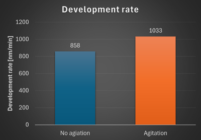
Testing showed that adding agitation to the puddle step gave better uniformity in the development rate over the entire area of the substrate as well as increased development rate.
Tests were performed on under-exposed resist, specifically for showing the difference between the agitation and non-agitation puddle development - the measured results cannot necessarily be transferred directly to a working process, only the vague general behavior of the two process setups; faster/slower development speed and better/worse uniformity across substrate.


| Non-agitation | Agitation | |
|---|---|---|
| Test results |
|
|
| Normalized development rate | 1 | 1.20 |
| Non-uniformity | 21% | 11% |
| Agitation | None | 15 cycles per minute, 20 rpm, 500 rpm/s |
| Substrate | 100 mm SSP silicon | |
| Resist film | 1.5 µm AZ 5214E | |
| Exposure dose | 50 mJ/cm2 (~50% of normal dose) | |
| Development | Single puddle for 60 seconds | |
| Developer | AZ 726 MIF (2.38% TMAH) | |
