Specific Process Knowledge/Characterization/MicroSpectroPhotometer (Craic 20/30 PV): Difference between revisions
| Line 280: | Line 280: | ||
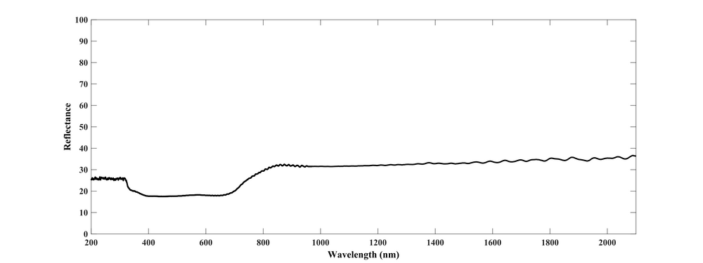
image:eves_CRAIC_reflectance_Si_ssp_20231002.png|Reflectance measurement of a Si (ssp, n-doped) wafer. Standard CRAIC Al sample was used as a reference. Objective 10X, Aperture number: 2. | image:eves_CRAIC_reflectance_Si_ssp_20231002.png|Reflectance measurement of a Si (ssp, n-doped) wafer. Standard CRAIC Al sample was used as a reference. Objective 10X, Aperture number: 2. | ||
image:eves_CRAIC_reflectance_fused_silica_reference_20231002.png|Reflectance measurement of a fused silica wafer piece. Standard CRAIC Al sample was used as a reference. Objective 10X, Aperture number: 2. | image:eves_CRAIC_reflectance_fused_silica_reference_20231002.png|Reflectance measurement of a fused silica wafer piece. Standard CRAIC Al sample was used as a reference. Objective 10X, Aperture number: 2. | ||
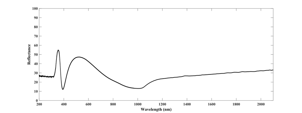
image:eves_CRAIC_reflectance_TiO2_150C_2161cycles_refl_20231002.png|Reflectance measurement of TiO2 deposited at 150C and 2161 cycles (ca. 100nm) on a ssp Si using ALD. Standard CRAIC Al sample was used as a reference. Objective 10X, Aperture number: 2. | image:eves_CRAIC_reflectance_TiO2_150C_2161cycles_refl_20231002.png|Reflectance measurement of TiO2 deposited at 150C and 2161 cycles (ca. 100nm) on a ssp Si using [[Specific_Process_Knowledge/Thin_film_deposition/ALD_Picosun_R200|ALD]]. Standard CRAIC Al sample was used as a reference. Objective 10X, Aperture number: 2. | ||
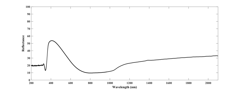
image:eves_CRAIC_reflectance_TiO2_350C_2174cycles_refl_20231002.png|Reflectance measurement of TiO2 deposited at 350C and 2174 cycles (ca. 100nm) on a ssp Si using ALD. Standard CRAIC Al sample was used as a reference. Objective 10X, Aperture number: 2. | image:eves_CRAIC_reflectance_TiO2_350C_2174cycles_refl_20231002.png|Reflectance measurement of [[Specific_Process_Knowledge/Thin_film_deposition/ALD_Picosun_R200/TiO2_deposition_using_ALD|TiO2]] deposited at 350C and 2174 cycles (ca. 100nm) on a ssp Si using [[Specific_Process_Knowledge/Thin_film_deposition/ALD_Picosun_R200|ALD]]. Standard CRAIC Al sample was used as a reference. Objective 10X, Aperture number: 2. | ||
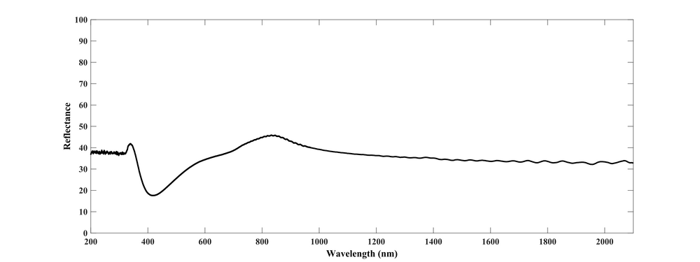
image:eves_CRAIC_reflectance_AlN_20231002.png|Reflectance measurement of 127 nm AlN deposited on a ssp 6" Si using reactive sputtering method. Standard CRAIC Al sample was used as a reference. Objective 10X, Aperture number: 2. | image:eves_CRAIC_reflectance_AlN_20231002.png|Reflectance measurement of 127 nm AlN deposited on a ssp 6" Si using reactive sputtering method. Standard CRAIC Al sample was used as a reference. Objective 10X, Aperture number: 2. | ||
image:eves_CRAIC_reflectance_Alu_TiO_5x5nm_10bilayer_on_Si_20231002.png|Reflectance measurement of alumina-titania stack of total thickness of 100nm deposited on a ssp Si using ALD. Each layer is 5nm, so 10 bilayers in total. Standard CRAIC Al sample was used as a reference. Objective 10X, Aperture number: 2. | image:eves_CRAIC_reflectance_Alu_TiO_5x5nm_10bilayer_on_Si_20231002.png|Reflectance measurement of alumina-titania stack of total thickness of 100nm deposited on a ssp Si using [[Specific_Process_Knowledge/Thin_film_deposition/ALD_Picosun_R200|ALD]]. Each layer is 5nm, so 10 bilayers in total. Standard CRAIC Al sample was used as a reference. Objective 10X, Aperture number: 2. | ||
image:eves_CRAIC_reflectance_Alu_TiO_5x5nm_10bilayer_on_glass_20231002.png|Reflectance measurement of alumina-titania stack of total thickness of 100nm deposited on a fused silica wafer using ALD. Each layer is 5nm, so 10 bilayers in total. Standard CRAIC Al sample was used as a reference. Objective 10X, Aperture number: 2. | image:eves_CRAIC_reflectance_Alu_TiO_5x5nm_10bilayer_on_glass_20231002.png|Reflectance measurement of alumina-titania stack of total thickness of 100nm deposited on a fused silica wafer using [[Specific_Process_Knowledge/Thin_film_deposition/ALD_Picosun_R200|ALD]]. Each layer is 5nm, so 10 bilayers in total. Standard CRAIC Al sample was used as a reference. Objective 10X, Aperture number: 2. | ||
image:eves_CRAIC_reflectance_rmal_Au_APTMS_20231002.png|Reflectance measurement of Au layer deposited on fused silica wafer with [[Specific Process Knowledge/Thin film deposition/Deposition_of_Gold#Adhesion_of_Au_on_Si|APTMS as adhesion layer]]. Standard CRAIC Al sample was used as a reference. Objective 10X, Aperture number: 2. | image:eves_CRAIC_reflectance_rmal_Au_APTMS_20231002.png|Reflectance measurement of Au layer deposited on fused silica wafer with [[Specific Process Knowledge/Thin film deposition/Deposition_of_Gold#Adhesion_of_Au_on_Si|APTMS as adhesion layer]]. Standard CRAIC Al sample was used as a reference. Objective 10X, Aperture number: 2. | ||
image:eves_CRAIC_reflectance_Au_200nm_20231002.png|Reflectance measurement of 200nm Au layer deposited on ssp Si with 2 nm Cr as adhesion layer. Standard CRAIC Al sample was used as a reference. Objective 10X, Aperture number: 2. | image:eves_CRAIC_reflectance_Au_200nm_20231002.png|Reflectance measurement of 200nm Au layer deposited on ssp Si with 2 nm Cr as adhesion layer. Standard CRAIC Al sample was used as a reference. Objective 10X, Aperture number: 2. | ||
Revision as of 17:49, 9 November 2023
Feedback to this page: click here
Unless otherwise stated, all content on this page was created by Evgeniy Shkondin (DTU Nanolab)
All images and photos on this page belongs to DTU Nanolab.
Microspectrophotometer (Craic 20/30 PV)
- Microspectrophotometer.
-
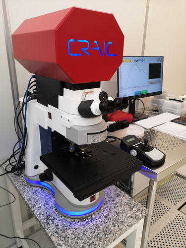 Craic 20/30 PV.

We acquired a microspectrophotometer, the CRAIC 20/30 PV, in 2021. This advanced instrument is designed for precise measurements of reflectance, transmission, and absorbance of thin films and microstructures within the UV/Visible/NIR wavelength range, spanning from 480nm to 1698nm.
This microspectrophotometer boasts two dedicated spectrometers: one for UV-Visible (200-900nm) and another for NIR (900-2230nm). It delivers exceptional spectral resolution, with 0.5 nm for the UV/Visible detector and 3.0 nm for the NIR detector. Importantly, the system allows for the separate storage of measured spectra and offers customizable merging of the two spectra.
Equipped with two objectives, a 10x quartz objective (wavelength range 220 nm to 2100 nm, NA 0.2, WD 7.4 mm) and a 40x quartz objective (wavelength range 240 nm to 2100 nm, NA 0.6, WD 0.36 mm), this tool provides versatility for various applications. Six aperture sizes, ranging from 100.2 to 1.5 microns, can be selected depending on the objective, facilitating the characterization of micro- and nanostructures' optical properties.
For polarization measurements, polarizers and analyzers can be installed as needed. An intriguing feature is the motorized stage, offering a generous movement range of 114 mm by 75 mm, with a precise 0.02 µm step size. This enables comprehensive sample mapping.
The microspectrophotometer operates as follows: A microscope-mounted lamp emits white light focused onto the sample. The sample selectively absorbs specific wavelengths, dependent on its chromophore's chemical structure and environment. Unabsorbed light is collected by the microspectrophotometer objective, focused onto the spectrophotometer's entrance aperture. The mirrored aperture reflects most of the light into a digital imaging system, simplifying alignment and spectrum acquisition.
The remaining unreflected light passes through the aperture into the spectrophotometer, where an optical grating separates it into component wavelengths. These wavelengths are measured by a pixel on a Charge Coupled Device (CCD) detector. The data is stored and presented as an optical spectrum, visualized as an XY chart displaying intensity at each wavelength.
Various microspectroscopy techniques are employed based on sample characteristics. For instance, opaque samples are analyzed with incident or reflectance illumination, while transparent samples are examined using transmitted light. Our microspectrophotometer can be configured to measure transmission, absorbance, and reflectance spectra.
Operation is straightforward: First, a dark scan measures system dark counts. Then, a reference material's spectrum is collected, encompassing spectral characteristics of the reference material, light sources, optics, and the CCD. Finally, the sample's spectrum is acquired, and an algorithm calculates the appropriate spectra for the specific lighting conditions (e.g., reflectance spectra for incident illumination). This algorithm is applied automatically, with the result displayed as a spectrum.
In summary, our CRAIC 20/30 PV microspectrophotometer empowers precise and versatile spectral measurements across a wide wavelength range, catering to a broad spectrum of research needs.
Work principle
- Microspectrophotometer.
-
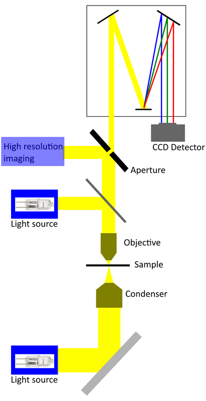 Light path in Craic 20/30 PV.

The term "microspectrophotometer" is often used interchangeably with "microscope spectrophotometer," but there are important distinctions between the two.
In essence, a microspectrophotometer is a purpose-built, fully integrated instrument that seamlessly combines an optical microscope with a highly sensitive spectrophotometer. This integration eliminates performance limitations typically associated with add-on components for standard microscopes.
To better understand this, let's break down the components:
Microscope:
A microscope is an optical device that utilizes lenses and mirrors to magnify microscopic objects or specific regions of larger objects. The sample under observation can be illuminated in several ways:
- Transmission Illumination: In this method, light is directed onto the sample through a condenser, and the portion that passes through the sample is collected by the microscope objective.
- Incident or Reflectance Illumination: Here, light is once again focused onto the sample through the objective, but this time, the reflected light from the sample is collected by the same objective. Reflectance illumination can be further categorized into specular and diffuse incident illumination.
The microscope objective plays a crucial role in collecting light from the sample and directing it towards the spectrophotometer's aperture. Simultaneously, a digital imaging system captures images of both the aperture and the sample, offering a real-time representation of what the spectrophotometer aperture is measuring.
Spectrophotometer:
The spectrophotometer is an optical instrument designed to measure light intensity across different wavelengths. In the microspectrophotometer, light collected from the sample enters through the aperture and passes through a diffraction grating, which disperses it into its constituent wavelengths. The separated light is then focused onto a CCD (Charge-Coupled Device) array detector, where each pixel of the array measures the intensity of a specific wavelength. The data is then transmitted to a computer, resulting in a spectrum that illustrates the intensity of each wavelength of light.
In the case of advanced microspectrophotometers like those manufactured by CRAIC Technologies, the spectrophotometer is seamlessly integrated with a specially designed microscope. This integration ensures that the microscope optics and light sources are of the highest quality, capable of operating across the ultraviolet, visible, and near-infrared spectrums (unlike standard microscopes, which are limited to the visible range).
Furthermore, the spectrophotometer is an integral part of the microscope, accompanied by a digital imaging system. This configuration maximizes light collection from even the tiniest samples. Consequently, microspectrophotometers are incredibly versatile instruments, capable of measuring absorbance, transmittance, reflectance, and emission spectra (including fluorescence) from samples as small as sub-micron in size.
Reflectance Calculation
Reflectance calculation involves the generation of a reflectance spectrum, which can be derived from either sample and reference single-beam spectra or from a log 1/R spectrum.
From Two Single-Beam Spectra: To create a reflectance spectrum from two single-beam spectra, you can use the following formula:
In this formula, R represents the single-beam spectrum of the reference material, S represents the single-beam spectrum of the sample, and D represents the dark counts of the system.
Transmittance Calculation
Transmittance calculation involves generating a transmission spectrum by comparing two single-beam spectra: one from the sample and the other from the reference.
This is accomplished using the following formula:
In this formula, R represents the single-beam spectrum of the reference material, S represents the single-beam spectrum of the sample, and D represents the dark counts of the system.
The transmission spectrum can be computed based on the absorbance data using the following formula:
Here, A represents the absorbance value, which is derived from previously gathered data.
Absorbance Calculation
Absorbance calculation involves the generation of an absorption spectrum, which can be derived either from sample and reference single-beam spectra or from a transmission spectrum.
From Two Single-Beam Spectra: To create an absorption spectrum from two single-beam spectra, you can use the following formula:
In this formula, R represents the single-beam spectrum of the reference material, S represents the single-beam spectrum of the sample, and D represents the dark counts of the system.
From Transmission Data: Alternatively, you can generate an absorption spectrum from transmission data using the following formula:
This formula allows you to convert percent transmittance (%T) values into absorbance. It is particularly useful for processing data that has already been collected.
Performance
- Wavelength range 200 nm to 1698 nm; (In reality, the shortest measurable wavelength is approximately 370 nm, primarily limited by the characteristics of the halogen light source. On the other end, the longest wavelength can be extended to 2100 nm, constrained by the objective of the measurement. Therefore, in practical terms, the achievable measurement wavelength range falls within 375-2100 nm.)
- Spectral resolution 0.5 nm for UV/VIS detector, 3.0 nm for NIR detector. (The measured spectra can be stored separately, and the merge window of the two spectra can be customized);
- Two objectives are installed on the system:
 10x quartz objective (wavelength range 220 nm to 2100 nm, NA 0.2, WD 7.4 mm);
 40x quartz objective (wavelength range 240 nm to 2100 nm, NA 0.6, WD 0.36 mm);
- The motorized stage has a movement range of 114 mm by 75 mm, with 0,02 µm step size
- Two spectrometers are installed on the system:
 Detector 1 (CACBS135) UV/VIS 151-1110 nm
 Detector 2 (NQLBN1008) NIR 694-2210 nm
| Technical specifications of the objectives | ||||||||||||||||||||||||||||
| ||||||||||||||||||||||||||||
| Aperture sizes for 10x and 40x objectives. | ||||||||||||||||||||||||||||||||||||||||
| ||||||||||||||||||||||||||||||||||||||||
Examples
Objective 10x with the Aperture number 2 (75.3µm x 75.3µm) has been used in all the following examples. Filter #2 was used for reflection, and #1 for transmittance.
-
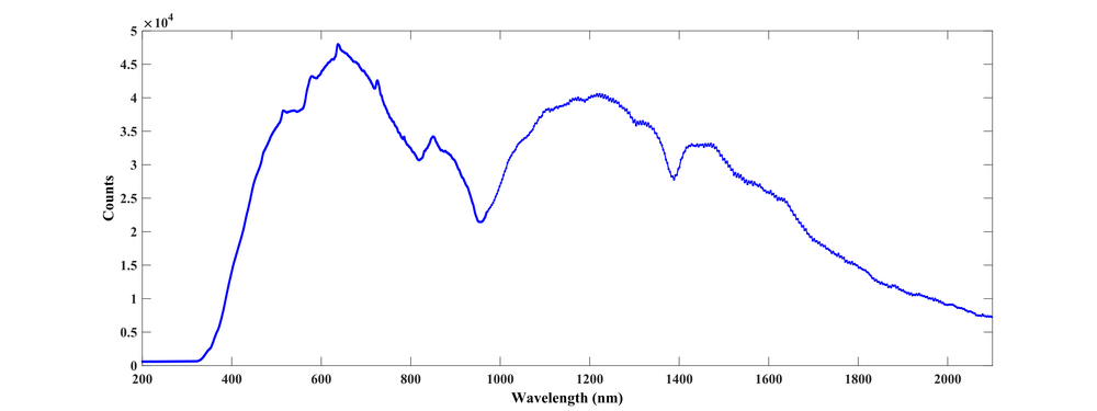 Counts from CRAIC Al reference sample. Collect dark and reference procedure result before reflectance measurements.
 -
 Counts from CRAIC quartz reference sample. Collect dark and reference procedure result before transmittance measurements.


Reflectance measurements
-
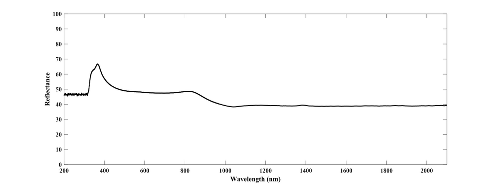 Reflectance measurement of a Si (ssp, n-doped) wafer. Standard CRAIC Al sample was used as a reference. Objective 10X, Aperture number: 2.
 -
 Reflectance measurement of a fused silica wafer piece. Standard CRAIC Al sample was used as a reference. Objective 10X, Aperture number: 2.
 -
 Reflectance measurement of TiO2 deposited at 150C and 2161 cycles (ca. 100nm) on a ssp Si using ALD. Standard CRAIC Al sample was used as a reference. Objective 10X, Aperture number: 2.
 -
-
 Reflectance measurement of 127 nm AlN deposited on a ssp 6" Si using reactive sputtering method. Standard CRAIC Al sample was used as a reference. Objective 10X, Aperture number: 2.
 -
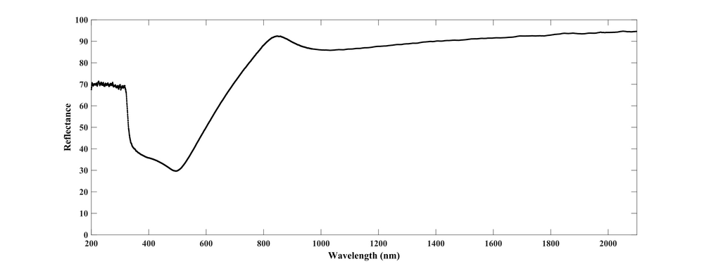
 Reflectance measurement of alumina-titania stack of total thickness of 100nm deposited on a ssp Si using ALD. Each layer is 5nm, so 10 bilayers in total. Standard CRAIC Al sample was used as a reference. Objective 10X, Aperture number: 2.
 -
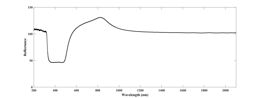
 Reflectance measurement of alumina-titania stack of total thickness of 100nm deposited on a fused silica wafer using ALD. Each layer is 5nm, so 10 bilayers in total. Standard CRAIC Al sample was used as a reference. Objective 10X, Aperture number: 2.
 -
 Reflectance measurement of Au layer deposited on fused silica wafer with APTMS as adhesion layer. Standard CRAIC Al sample was used as a reference. Objective 10X, Aperture number: 2.
 -
 Reflectance measurement of 200nm Au layer deposited on ssp Si with 2 nm Cr as adhesion layer. Standard CRAIC Al sample was used as a reference. Objective 10X, Aperture number: 2.


Transmittance measurements
-
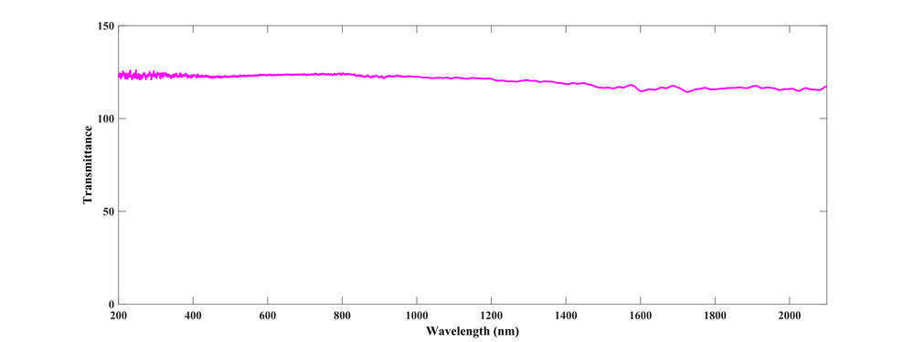 Transmittance measurement of a fused silica wafer. Standard CRAIC quartz sample was used as a reference. Objective 10X, Aperture number: 2.
 -
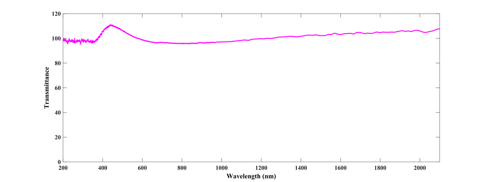 Transmittance measurement of an alumina-titania stack of total thickness of 100nm deposited on a fused silica wafer using ALD. Each layer is 5nm, so 10 bilayers in total. Standard CRAIC quartz sample was used as a reference. Objective 10X, Aperture number: 2.
 -
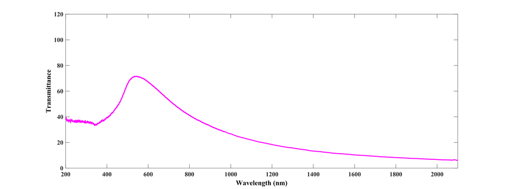 Transmittance measurement of Au layer deposited on fused silica wafer with APTMS as adhesion layer. Standard CRAIC quartz sample was used as a reference. Objective 10X, Aperture number: 2.


