Specific Process Knowledge/Etch/DRIE-Pegasus/Pegasus-3: Difference between revisions
| Line 10: | Line 10: | ||
<span style="background:#FF2800">THIS PAGE IS UNDER CONSTRUCTION</span>[[image:Under_construction.png|200px]] | |||
'''The tool is ready for user training. ''' | '''The tool is ready for user training. ''' | ||
Revision as of 12:52, 10 August 2021
Feedback to this page: click here
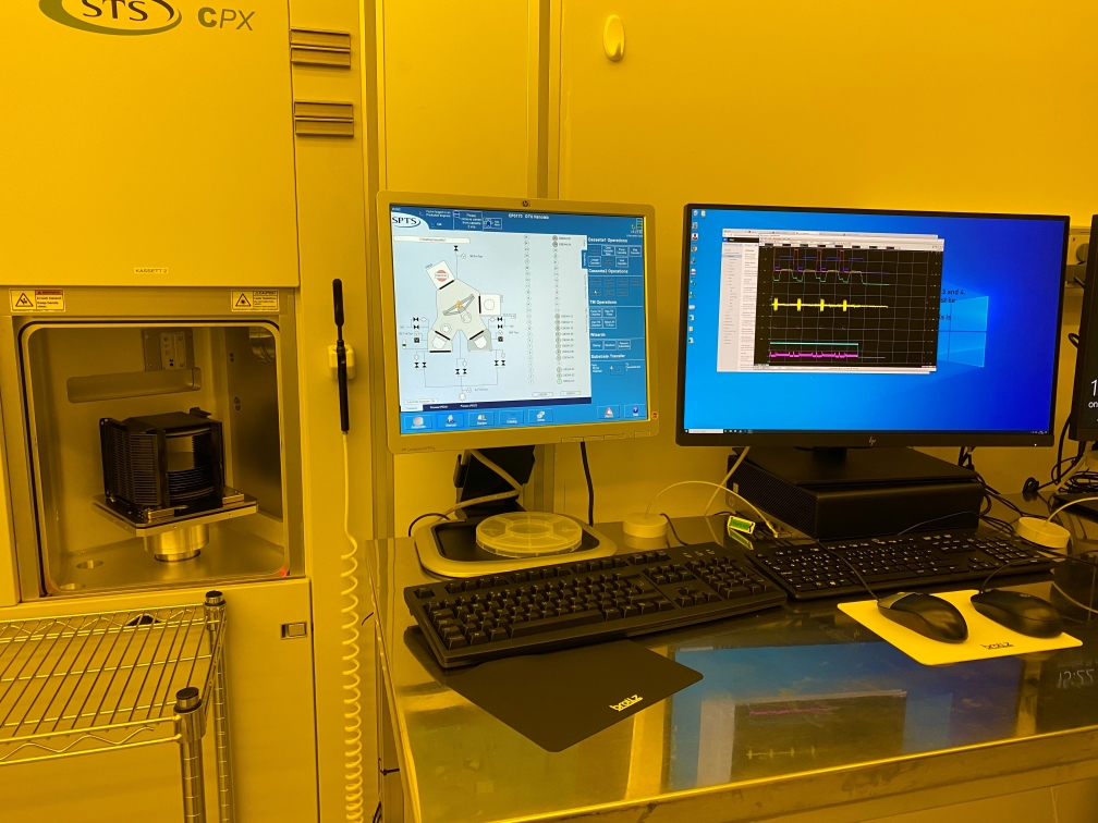
Pegasus 3 - 150mm silicon etching
THIS PAGE IS UNDER CONSTRUCTION
The tool is ready for user training.

The user manual(s) is available, technical information and contact information can be found in LabManager:
Equipment info in LabManager
Process information
Hardware changes
Compared to a standard SPTS DRIE Pegasus chamber, the Pegasus 3 has had the same modifications as the Pegasus 1 with the exception of the Claritas EPD system. The changes are listed below.
Other etch processes
More processes, such as for DUV resist, are currently being developed, but they are not quite 'ready for publication' at LabAdviser so please contact Jonas (mailto:jmli@dtu.dk) for more information.
Wafer bonding
To find information on how to bond wafers or chips to a carrier wafer, click here.
Internal Nanolab Process log for Pegasus 3
Process log at Nanolab [1]
