Specific Process Knowledge/Thin film deposition/Furnace LPCVD PolySilicon: Difference between revisions
No edit summary |
|||
| Line 127: | Line 127: | ||
|- | |- | ||
|} | |} | ||
== Rules for storage and RCA cleaning of wafers to the B2 and E4 furnaces == | |||
*[[Specific_Process_Knowledge/Thermal_Process/Storage_and_cleaning_of_wafer_to_the_A,_B,_C_and_E_stack_furnaces|Storage and cleaning of wafer to the B2 and E4 furnaces]] | |||
Revision as of 16:45, 3 December 2019
Feedback to this page: click here
Deposition of silicon using LPCVD


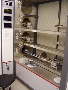
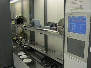
DTU Nanolab has two furnaces for deposition of LPCVD (Low Chemical Vapour Deposition) silicon: A 6" furnace (installed in 2011) for deposition of standard polySi, amorphous Si and boron doped polySi on 100 mm or 150 mm wafers and a 4" furnace (installed in 1995) for deposition of standard polySi, amorphous Si, boron- and phosphorous doped polySi on 100 mm wafers. In LabManager the two furnaces are named "Furnace: LPCVD Poly-Si (4") (B4)" and "Furnace: LPCVD Poly-Si (6") (E2)", respectively. Both furnaces are Tempress horizontal furnaces.
The LPCVD silicon deposition is a batch process, where silicon is deposited on a batch of 25 or 50 wafers (6" polySi furnace) or 30 wafers (4" polySi furnace). The silicon has a good step coverage, and especially for standard polySi the film thickness is very uniform over the wafers.
The reactive gas is silane (SiH4). The dopant for boron doped polySi is BCl3 - only available at request (6" polySi furnace) or B2H6 (4" polySi furnace), and for phosphorous doped polySi the dopant is PH3 (4" polySi furnace). For standard and doped polysilion the deposition takes place at a temperature of 600 oC - 620 oC and a pressure of 200-250 mTorr. For amorphous silicon the deposition temperature is lower, and thus the deposition rate is also lower. For phosphorus doped polySi the deposition rate is approximately ten times lower than for standard and boron doped polySi. Please check the cross contamination information in LabManager before you use any of the two furnaces.
The user manuals, quality control procedures and results, technical information and contact information can be found in LabManager:
4" LPCVD polysilicon furnace (B4)
6" LPCVD polysilicon furnace (E2)
Process information
- Deposition of polysilicon using the 4" polysilicon furnace
- Boron doped poly-Si and a-Si by using 4" polysilicon furnace
| Equipment | 4" LPCVD polysilicon furnace (B4) | 6" LPCVD polysilicon furnace (E2) | ||
|---|---|---|---|---|
| Purpose | Deposition of |
|
| |
| Performance | Step coverage |
|
| |
| Film quality |
|
| ||
| Process parameter range | Process Temperature |
|
The process temperature vary over the furnace tube | |
| Process pressure |
|
The process pressure depends on the process | ||
| Gas flows |
|
The silane (SiH4) flow depends on the process | ||
| Substrates | Batch size |
Including a testwafer with ~110 nm oxide |
Including a testwafer with ~110 nm oxide |
|
| Substrate materials allowed |
|
| ||
