Specific Process Knowledge/Etch/Wet Aluminium Etch: Difference between revisions
Appearance
| Line 21: | Line 21: | ||
<!-- remember to remove the type of documents that are not present --> | <!-- remember to remove the type of documents that are not present --> | ||
[http://labmanager.dtu.dk/function.php?module=Machine&view=view& | [http://labmanager.dtu.dk/function.php?module=Machine&view=view&mach=381 Al-etch info page in LabManager] | ||
==Comparing the two solutions== | ==Comparing the two solutions== | ||
Revision as of 15:11, 9 August 2017
THIS PAGE IS UNDER CONSTRUCTION
Feedback to this page: click here
Ething of Aluminium can be done either wet or dry. For wet etching please see below on this page. Dry etching can be done either with the ICP Metal Etch using Chlorine chemistry or with IBE by sputtering with Ar ions.
Wet Aluminium Etch

Wet etching of aluminium is done with two different solutions:
- H2O:H3PO4 1:2 at 50 oC
- Pre-mixed etch solution: PES 77-19-04 at 20 oC
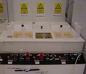
Both solutions are used in the Aluminium etch bath shown to the right. It must be written on which one is in. Solution no. 1 is the most used solution for etching aluminium. Solution no. 2 is primarily for etching aluminium mixed with a small percentage of silicon.
The user manual and contact information can be found in LabManager:
Al-etch info page in LabManager
Comparing the two solutions
| Aluminium Etch 1 | Aluminium Etch 2 | |
|---|---|---|
| General description | Etch of pure aluminium | Etch of aluminium + 1.5% Si |
| Link to KBA | ||
| Chemical solution | H2O:H3PO4 1:2 | PES 77-19-04
77 vol% H3PO4 85% 19 vol% CH3COOH 100% 4 vol% HNO3 70% |
| Process temperature! | 50 oC | 20 oC |
| Possible masking materials! | Photoresist (1.5 µm AZ5214E) | Photoresist (1.5 µm AZ5214E) |
| Etch rate | ~100 nm/min (Pure Al) | ~60 nm/min |
| Batch size! | 1-25 wafers at a time | 1-25 wafer at a time |
| Size of substrate | 4" wafers | 4" wafers |
| Allowed materials |
|
|
