Specific Process Knowledge/Etch/ICP Metal Etcher: Difference between revisions
Appearance
No edit summary |
|||
| (137 intermediate revisions by 5 users not shown) | |||
| Line 1: | Line 1: | ||
= | '''Feedback to this page''': '''[mailto:labadviser@nanolab.dtu.dk?Subject=Feed%20back%20from%20page%20http://labadviser.nanolab.dtu.dk/index.php/Specific_Process_Knowledge/Etch/ICP_Metal_Etcher click here]''' | ||
<!--Page reviewed by jmli 9/8-2022 --> | |||
<!--Checked for updates on 4/9-2025 - ok/jmli --> | |||
[[Category: Equipment |Etch ICP Metal]] | |||
[[Category: Etch (Dry) Equipment|ICP metal]] | |||
== The ICP Metal Etcher == | |||
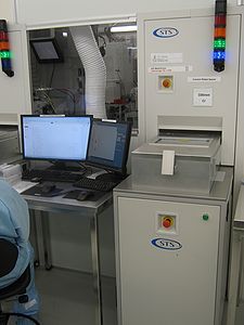
[[Image:ICP-Metal-Etcher.jpg |300x300px|thumb|The SPTS ICP Metal Etcher in the DTU Nanolab cleanroom B-1]] | |||
Name: PRO ICP <br> | |||
Vendor: STS (now SPTS) <br> | |||
The ICP Metal Etcher allows you to dry etch a small set of metals that includes aluminium, titanium, chromium, titanium tungsten and molybdenum (along with the related oxides and nitrides). It is, despite its name, strictly forbidden to etch (or expose to plasma) other metals. In order to do so use the [[Specific Process Knowledge/Etch/IBE⁄IBSD Ionfab 300|IBE/IBSD Ionfab 300]]. | |||
'''The user manual, user APV and contact information can be found in LabManager:''' | |||
Equipment info in [http://labmanager.dtu.dk/function.php?module=Machine&view=view&mach=266 LabManager] | |||
==Process information== | |||
'''Standard recipes''' | |||
*[[Specific Process Knowledge/Etch/ICP Metal Etcher/Aluminium|Etch of aluminium]] | |||
*[[Specific Process Knowledge/Etch/ICP Metal Etcher/Titanium|Etch of titanium]] | |||
*[[Specific Process Knowledge/Etch/ICP Metal Etcher/Chromium|Etch of chromium]] | |||
'''Other etch recipes''' | |||
*[[Specific Process Knowledge/Etch/ICP Metal Etcher/Barc Etch|Barc Etch]] | |||
*[[Specific Process Knowledge/Etch/ICP Metal Etcher/silicon|Etch of silicon]] | |||
*[[Specific Process Knowledge/Etch/ICP Metal Etcher/silicon oxide|Etch of silicon oxide]] | |||
*[[Specific Process Knowledge/Etch/ICP Metal Etcher/silicon nitride|Etch of silicon nitride]] | |||
*[[Specific Process Knowledge/Etch/Titanium Oxide/ICP metal|Etch of Titanium Oxide]] | |||
*[[Specific Process Knowledge/Etch/Titanium Nitride/ICP metal|Etch of Titanium Nitride]] | |||
*[[Specific Process Knowledge/Etch/Aluminum Oxide/Al2O3 Etch with ICP Metal|Al<sub>2</sub>O<sub>3</sub> Etch]] | |||
'''End point detection''' | |||
*[[/Examples of End point detection|Examples of End point detection]] | |||
==An overview of the performance of the ICP Metal Etcher and some process related parameters== | |||
{| border="2" cellspacing="0" cellpadding="2" | |||
|- | |- | ||
! | !style="background:silver; color:black;" align="left"|Purpose | ||
|style="background:LightGrey; color:black"|Dry etch of | |||
| | |style="background:WhiteSmoke; color:black"| | ||
| | * Metals such as aluminium, chromium and titanium and the related oxides and nitrides | ||
| | * Metals such as molybdenum, tungsten, titanium tungsten | ||
| | |||
| | |||
|- | |- | ||
! | !style="background:silver; color:black" align="left" valign="top" rowspan="2"|Performance | ||
| | |style="background:LightGrey; color:black"|Etch rates | ||
| | |style="background:WhiteSmoke; color:black"| | ||
| | * Aluminium : ~350 nm/min (depending on features size and etch load) | ||
| | |||
| | |||
|- | |- | ||
|style="background:LightGrey; color:black"|Anisotropy | |||
|style="background:WhiteSmoke; color:black"| | |||
*Good | |||
| | |||
| | |||
| | |||
| | |||
|- | |- | ||
! | !style="background:silver; color:black" align="left" valign="top" rowspan="2"|Process parameter range | ||
|style="background:LightGrey; color:black"|Process pressure | |||
|style="background:WhiteSmoke; color:black"| | |||
*~0.1-95 mTorr | |||
| | |||
| | |||
| | |||
| | |||
| | |||
|- | |- | ||
|style="background:LightGrey; color:black"|Gas flows | |||
| | |style="background:WhiteSmoke; color:black"| | ||
| | {| | ||
| | | SF<sub>6</sub>: 0-100 sccm | ||
| O<sub>2</sub>: 0-100 sccm | |||
| | |||
| | |||
| | |||
| | |||
|- | |- | ||
| C<sub>4</sub>F<sub>8</sub>: 0-100 sccm | |||
| Ar: 0-300 sccm | |||
| | |||
| | |||
|- | |- | ||
| CF<sub>4</sub>: 0-100 sccm | |||
| | | H<sub>2</sub>: 0-30 sccm | ||
|- | |- | ||
| CH<sub>4</sub>: not working | |||
| | | BCl<sub>3</sub>: 0-90 sccm | ||
|90 | |||
|- | |- | ||
| Cl<sub>2</sub>: 0-100 sccm | |||
| HBr: 0-100 sccm | |||
|- | |} | ||
|- | |||
| | |||
|- | |- | ||
! | !style="background:silver; color:black" align="left" valign="top" rowspan="3"|Substrates | ||
|style="background:LightGrey; color:black"|Batch size | |||
|style="background:WhiteSmoke; color:black"| | |||
*1 6" wafer per run | |||
*1 4" wafer per run | |||
*1 2" wafer per run | |||
*Or several smaller pieces on a carrier wafer | |||
| | |||
| | |||
| | |||
|- | |- | ||
| style="background:LightGrey; color:black"|Substrate material allowed | |||
|style="background:WhiteSmoke; color:black"| | |||
*Silicon wafers | |||
**with layers of silicon oxide or silicon (oxy)nitride | |||
*Quartz wafers | |||
|- | |||
| style="background:LightGrey; color:black"|Possible masking material | |||
|style="background:WhiteSmoke; color:black"| | |||
*Photoresist/e-beam resist | |||
*PolySilicon, Silicon oxide or silicon (oxy)nitride | |||
*Aluminium, titanium or chromium | |||
|- | |||
|} | |} | ||
Latest revision as of 10:32, 4 September 2025
Feedback to this page: click here
The ICP Metal Etcher

Name: PRO ICP
Vendor: STS (now SPTS)
The ICP Metal Etcher allows you to dry etch a small set of metals that includes aluminium, titanium, chromium, titanium tungsten and molybdenum (along with the related oxides and nitrides). It is, despite its name, strictly forbidden to etch (or expose to plasma) other metals. In order to do so use the IBE/IBSD Ionfab 300.
The user manual, user APV and contact information can be found in LabManager:
Equipment info in LabManager
Process information
Standard recipes
Other etch recipes
- Barc Etch
- Etch of silicon
- Etch of silicon oxide
- Etch of silicon nitride
- Etch of Titanium Oxide
- Etch of Titanium Nitride
- Al2O3 Etch
End point detection
| Purpose | Dry etch of |
| |||||||||
|---|---|---|---|---|---|---|---|---|---|---|---|
| Performance | Etch rates |
| |||||||||
| Anisotropy |
| ||||||||||
| Process parameter range | Process pressure |
| |||||||||
| Gas flows |
| ||||||||||
| Substrates | Batch size |
| |||||||||
| Substrate material allowed |
| ||||||||||
| Possible masking material |
|
