
Specific Process Knowledge/Etch/KOH Etch: Difference between revisions
No edit summary |
|||
| (16 intermediate revisions by 4 users not shown) | |||
| Line 6: | Line 6: | ||
[[Category: Equipment|Etch Wet KOH etch]] | [[Category:Equipment|Etch Wet KOH etch]] | ||
[[Category: Etch (Wet) bath|KOH etch]] | [[Category:Etch (Wet) bath|KOH etch]] | ||
==Si etch - ''Anisotropic silicon etch''== | ==Si etch - ''Anisotropic silicon etch''== | ||
| Line 13: | Line 13: | ||
KOH belongs to the family of anisotropic Si-etchants based on aqueous alkaline solutions. The anisotropy stems from the different etch rates in different crystal directions. The {111}-planes are almost inert whereas the etch rates of e.g. {100}- and {110}-planes are several orders of magnitude faster. | KOH belongs to the family of anisotropic Si-etchants based on aqueous alkaline solutions. The anisotropy stems from the different etch rates in different crystal directions. The {111}-planes are almost inert whereas the etch rates of e.g. {100}- and {110}-planes are several orders of magnitude faster. | ||
KOH-etching is a highly versatile and cheap way to realize micro mechanical structures if you can live with the necessary Si<sub>3</sub>N<sub>4</sub>- or SiO<sub>2</sub>-masking materials and the potassium contamination of the surface. '''The latter necessitates in most cases a wet post-clean ([[Specific Process Knowledge/Wafer cleaning/7-up & Piranha|'7-up']] or [[Specific Process Knowledge/Wafer cleaning/RCA|RCA-clean]]) if the wafer is to be processed further.''' | KOH-etching is a highly versatile and cheap way to realize micro mechanical structures if you can live with the necessary Si<sub>3</sub>N<sub>4</sub>- or SiO<sub>2</sub>-masking materials and the potassium contamination of the surface. '''The latter necessitates in most cases a wet post-clean ([[Specific Process Knowledge/Wafer cleaning/7-up & Piranha|'7-up']] or [[Specific Process Knowledge/Wafer cleaning/RCA|RCA-clean]]) if the wafer is to be processed further. we also recommend to rinse the wafers in a 5% HCL solution to remove metal ions from the KOH solution.''' | ||
At DTU Nanolab we use as a standard a 28 wt% KOH. The etch rate - and the selectivity towards a SiO<sub>2</sub>-mask - is depending on the temperature. We normally use T=80 <sup>o</sup>C but may choose to reduce this to e.g. 60 <sup>o</sup>C or 70 <sup>o</sup>C in case of a high-precision timed etch (e.g. defining a thin membrane). In some cases we recommend to saturate the standard 28 wt% KOH with IPA with an etch temperature at T=70 <sup>o</sup>C (reduce evaporation of IPA). One example is for boron etch-stop, where the selectivity towards the boron-doped silicon is improved compared to the standard etch. Etching with IPA added to the KOH solution (250ml IPA/1000ml KOH) can be done in KOH fumehood. | At DTU Nanolab we use as a standard a 28 wt% KOH. The etch rate - and the selectivity towards a SiO<sub>2</sub>-mask - is depending on the temperature. We normally use T=80 <sup>o</sup>C but may choose to reduce this to e.g. 60 <sup>o</sup>C or 70 <sup>o</sup>C in case of a high-precision timed etch (e.g. defining a thin membrane). In some cases we recommend to saturate the standard 28 wt% KOH with IPA with an etch temperature at T=70 <sup>o</sup>C (reduce evaporation of IPA). One example is for boron etch-stop, where the selectivity towards the boron-doped silicon is improved compared to the standard etch. Etching with IPA added to the KOH solution (250ml IPA/1000ml KOH) can be done in KOH fumehood. | ||
| Line 21: | Line 21: | ||
<gallery caption="Different places to do anisotropic wet silicon etch" widths="350px" heights="250px" perrow="3"> | <gallery caption="Different places to do anisotropic wet silicon etch" widths="350px" heights="250px" perrow="3"> | ||
image:KOH_BHF.JPG|Wetbench 01: Si etch, for Si etch of 4" and 6" wafers using KOH. Positioned in cleanroom D-3. | image:KOH_BHF.JPG|Wetbench 01: Si etch, for Si etch of 4" and 6" wafers using KOH. Positioned in cleanroom D-3. | ||
image:KOH_fumehood.JPG|Fume hood 06: Si etch, for Si etch of 4" and 6" wafers using KOH. Positioned in cleanroom D-3. This is used for wafers that are considered dirty.</gallery> | image:KOH_fumehood.JPG|Fume hood 06: Si etch, for Si etch of 4" and 6" wafers using KOH. Positioned in cleanroom D-3. This is used for wafers that are considered dirty. The workspace in the fume hood can also be booked and used for beaker etch of Si and in some cases Chromium etch.</gallery> | ||
'''The user manuals, quality control procedures and results, user APVs, technical information and contact information can be found in LabManager:''' | '''The user manuals, quality control procedures and results, user APVs, technical information and contact information can be found in LabManager:''' | ||
| Line 43: | Line 43: | ||
Key facts for the different etch baths available at DTU Nanolab are resumed in the table: | Key facts for the different etch baths available at DTU Nanolab are resumed in the table: | ||
<br clear="all" /> | <br clear="all" /> | ||
{| border="2" cellspacing="0" cellpadding="2" | {| border="2" cellspacing="0" cellpadding="2" | ||
| Line 61: | Line 59: | ||
|style="background:WhiteSmoke; color:black"| | |style="background:WhiteSmoke; color:black"| | ||
*Etch of Silicon in 28 wt% KOH | *Etch of Silicon in 28 wt% KOH | ||
The bath is dedicated | The bath is dedicated wafers with metal or otherwise dirty wafers | ||
|- | |- | ||
|style="background:LightGrey; color:black"|Link to safety APV and SDS | |style="background:LightGrey; color:black"|Link to safety APV and SDS | ||
| Line 74: | Line 72: | ||
*:[http://kemibrug.dk/KBA/CAS/106882/?show_KBA=1&portaldesign=1 see SDS here] | *:[http://kemibrug.dk/KBA/CAS/106882/?show_KBA=1&portaldesign=1 see SDS here] | ||
|- | |- | ||
!style="background:silver; color:black" align="center" valign="center | ! rowspan="8" style="background:silver; color:black" align="center" valign="center" |Performance | ||
|style="background:LightGrey; color:black"|Etch rates in crystalline silicon (100) | |style="background:LightGrey; color:black"|Etch rates in crystalline silicon (100) | ||
|style="background:WhiteSmoke; color:black"| | |style="background:WhiteSmoke; color:black"| | ||
| Line 101: | Line 99: | ||
*Theoretical values: | *Theoretical values: | ||
*1.2 nm/min (60 °C) | *1.2 nm/min (60 °C) | ||
* | *7.5 nm/min (80 °C) | ||
|style="background:WhiteSmoke; color:black"| | |style="background:WhiteSmoke; color:black"| | ||
*Theoretical values: | *Theoretical values: | ||
*1.2 nm/min (60 °C) | *1.2 nm/min (60 °C) | ||
* | *7.5 nm/min (80 °C) | ||
|style="background:WhiteSmoke; color:black"| | |style="background:WhiteSmoke; color:black"| | ||
*Theoretical values: | *Theoretical values: | ||
*1.2 nm/min (60 °C) | *1.2 nm/min (60 °C) | ||
* | *7.5 nm/min (80 °C) | ||
|- | |- | ||
|style="background:LightGrey; color:black"|Etch rates in other oxides | |style="background:LightGrey; color:black"|Etch rates in other oxides | ||
| Line 120: | Line 118: | ||
*TEOS oxide from furnace: 300nm etched in 11 min | *TEOS oxide from furnace: 300nm etched in 11 min | ||
jemafh@nilt 2019-Marts: | jemafh@nilt 2019-Marts: | ||
*Standard from PECVD3: selectivity 1:100 to Si | *Standard from PECVD3: selectivity 1:100 to Si(100) | ||
|style="background:WhiteSmoke; color:black"| | |style="background:WhiteSmoke; color:black"| | ||
. | . | ||
|- | |- | ||
|style="background:LightGrey; color:black"|Etch rates in PECVD SiN | |style="background:LightGrey; color:black"|Etch rates in PECVD SiN | ||
|style="background:WhiteSmoke; color:black"| | |style="background:WhiteSmoke; color:black"| | ||
|style="background:WhiteSmoke; color:black"|See etchrates for PECVD SiN [https://labadviser.nanolab.dtu.dk/index.php?title=Specific_Process_Knowledge/Thin_film_deposition/Deposition_of_Silicon_Nitride/Deposition_of_Silicon_Nitride_using_PECVD/PECVD3:_Low_stress_nitride_testing#DOE_made_to_find_a_good_QC_nitride_recipe_with_low_stress_and_low_KOH_etch_rate_(by_Berit_Herstrøm_@_DTU_Nanolab_2016_Marts) here] | |||
|style="background:WhiteSmoke; color:black"| | |||
|- | |||
|style="background:LightGrey; color:black"|Etch rates in LPCVD Si3N4 and SiN | |||
|style="background:WhiteSmoke; color:black"| | |||
*Etch rates in LPCVD nitrides is very low. Etch selectivities to Si(100) is higher than 1:10.000 | |||
|style="background:WhiteSmoke; color:black"| | |||
*Etch rates in LPCVD nitrides is very low. Etch selectivities to Si(100) is higher than 1:10.000 | |||
|style="background:WhiteSmoke; color:black"| | |||
*Etch rates in LPCVD nitrides is very low. Etch selectivities to Si(100) is higher than 1:10.000 | |||
|- | |- | ||
|style="background:LightGrey; color:black"|Roughness | |style="background:LightGrey; color:black"|Roughness | ||
| Line 152: | Line 158: | ||
|style="background:WhiteSmoke; color:black"| | |style="background:WhiteSmoke; color:black"| | ||
*Mixing ratios giving 28 wt% KOH solutions | *Mixing ratios giving 28 wt% KOH solutions | ||
KOH:H<sub>2</sub>O - 1000 ml: 1200 ml, when using premixed 50% KOH solution | KOH:H<sub>2</sub>O - 1000 ml: 1200 ml, when using premixed 50% KOH solution | ||
|style="background:WhiteSmoke; color:black"| | |style="background:WhiteSmoke; color:black"| | ||
* | *Mixing ratios giving 28 wt% KOH solutions | ||
KOH:H<sub>2</sub>O - 1000 ml: 1200 ml, when using premixed 50% KOH solution | |||
|- | |- | ||
|style="background:LightGrey; color:black"|Temperature | |style="background:LightGrey; color:black"|Temperature | ||
Latest revision as of 13:55, 15 September 2026
Feedback to this page: click here
Unless anything else is stated, everything on this page, text and pictures are made by DTU Nanolab.
All links to Kemibrug (SDS) and Labmanager Including APV and QC requires login.
Si etch - Anisotropic silicon etch
KOH belongs to the family of anisotropic Si-etchants based on aqueous alkaline solutions. The anisotropy stems from the different etch rates in different crystal directions. The {111}-planes are almost inert whereas the etch rates of e.g. {100}- and {110}-planes are several orders of magnitude faster.
KOH-etching is a highly versatile and cheap way to realize micro mechanical structures if you can live with the necessary Si3N4- or SiO2-masking materials and the potassium contamination of the surface. The latter necessitates in most cases a wet post-clean ('7-up' or RCA-clean) if the wafer is to be processed further. we also recommend to rinse the wafers in a 5% HCL solution to remove metal ions from the KOH solution.
At DTU Nanolab we use as a standard a 28 wt% KOH. The etch rate - and the selectivity towards a SiO2-mask - is depending on the temperature. We normally use T=80 oC but may choose to reduce this to e.g. 60 oC or 70 oC in case of a high-precision timed etch (e.g. defining a thin membrane). In some cases we recommend to saturate the standard 28 wt% KOH with IPA with an etch temperature at T=70 oC (reduce evaporation of IPA). One example is for boron etch-stop, where the selectivity towards the boron-doped silicon is improved compared to the standard etch. Etching with IPA added to the KOH solution (250ml IPA/1000ml KOH) can be done in KOH fumehood.
- Different places to do anisotropic wet silicon etch
-
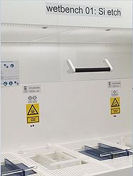 Wetbench 01: Si etch, for Si etch of 4" and 6" wafers using KOH. Positioned in cleanroom D-3.
 -
 Fume hood 06: Si etch, for Si etch of 4" and 6" wafers using KOH. Positioned in cleanroom D-3. This is used for wafers that are considered dirty. The workspace in the fume hood can also be booked and used for beaker etch of Si and in some cases Chromium etch.


The user manuals, quality control procedures and results, user APVs, technical information and contact information can be found in LabManager:
Si Etch 1: KOH info page in LabManager,
Si Etch 2: KOH info page in LabManager,
Si Etch 3: KOH info page in LabManager
Process Information
KOH etching baths
Key facts for the different etch baths available at DTU Nanolab are resumed in the table:
| Equipment | Si Etch 01: KOH | Si Etch 02: KOH | Si Etch 03: KOH | |
|---|---|---|---|---|
| Purpose |
|
|
|
The bath is dedicated wafers with metal or otherwise dirty wafers |
| Link to safety APV and SDS | ||||
| Performance | Etch rates in crystalline silicon (100) |
|
|
|
| Etch rates in crystalline silicon (110) |
|
|
| |
| Etch rates in Thermal SiO2 |
|
|
| |
| Etch rates in other oxides |
. |
yannickseis@nbi.ku nov. 2017 @80 °C:
jemafh@nilt 2019-Marts:
|
. | |
| Etch rates in PECVD SiN | See etchrates for PECVD SiN here | |||
| Etch rates in LPCVD Si3N4 and SiN |
|
|
| |
| Roughness |
|
|
| |
| Anisotropy |
|
|
| |
| Process parameter range | Chemical solution |
KOH:H2O - 1000 ml: 1200 ml, when using premixed 50% KOH solution |
KOH:H2O - 1000 ml: 1200 ml, when using premixed 50% KOH solution |
KOH:H2O - 1000 ml: 1200 ml, when using premixed 50% KOH solution |
| Temperature |
|
|
| |
| Substrates | Batch size |
|
|
|
| Size of substrate |
|
|
| |
| Allowed materials |
|
|
| |
| Masking material |
|
|
| |
1 Measured by Eric Jensen from DTU-Nanotech, October 2013.