Specific Process Knowledge/Etch/III-V ICP/InP-InGaAsP-InGaAs: Difference between revisions
| Line 263: | Line 263: | ||
Image:S0_oxide_05.jpg|Sample S0: Top view of the oxide mask before etching. It is the TRAVKA50 mask, but it is clear that the CD reduction is about the 1-1.5 µm of the lines. | Image:S0_oxide_05.jpg|Sample S0: Top view of the oxide mask before etching. It is the TRAVKA50 mask, but it is clear that the CD reduction is about the 1-1.5 µm of the lines. | ||
Image:S4_06.jpg|Sample S4: Profile view. The recipe InP etch has been used. <br> The sample has been run on a SiO2 carrier wafer. <br> There is not much CD change compared to the oxide mask before the etch. <br> It seems like the SiO2 mask is gone and the sidewall angle from the mask has been transferred into the sample. <br> The sidewall profile is quit vertical in the lower part. <br> Etch time 15 min <br> Etch depth in large open areas: 9.19µm | Image:S4_06.jpg|Sample S4: Profile view. The recipe InP etch has been used. <br> The sample has been run on a SiO2 carrier wafer. <br> There is not much CD change compared to the oxide mask before the etch. <br> It seems like the SiO2 mask is gone and the sidewall angle from the mask has been transferred into the sample. <br> The sidewall profile is quit vertical in the lower part. <br> Etch time 15 min <br> Etch depth in large open areas: 9.19µm | ||
Image:S5_05.jpg|Sample S5: Profile view. The recipe InP etch has been used but with modified Cl2 and N2 flows: N2=30 sccm Cl2=30 sccm. <br> The sample has been run on a SiO2 carrier wafer. <br> There is not much CD change compared to the oxide mask before the etch. <br> It seems like the SiO2 mask is gone. <br> The sidewall profile is overcutting probably due to too little passivation. <br> Etch time 10 min <br> Etch depth in large open areas: 11.82µm | Image:S5_05.jpg|Sample S5: Profile view. The recipe InP etch has been used but with modified Cl2 and N2 flows: N2=30 sccm Cl2=30 sccm. <br> The sample has been run on a SiO2 carrier wafer. <br> There is not much CD change compared to the oxide mask before the etch. <br> It seems like the SiO2 mask is gone. <br> The sidewall profile is overcutting probably due to too little passivation. <br> Etch time 10 min <br> Etch depth in large open areas: 11.82µm | ||
Latest revision as of 08:51, 10 March 2025
Feedback to this page: click here
InP etch with HBr chemistry (2019)
Work done by Aurimas Sakanas @Fotonik.dtu 2019. This work was done to obtain very low surface roughness.
| Recipe name | ? |
| HBr flow | 10 sccm |
| CH4 flow | 5 sccm |
| Ar flow | 2 sccm |
| Platen power | 50 W |
| Coil power | 600 W |
| Pressure | 5 mTorr |
| Platen chiller temperature | 180 oC |
| Comment | Sample crystal bonded (Crystalbond 509, clear color) to Si carrier |
| Results | |
| Etch rate |
250-350 nm/min (2" wafer) |
| Sidewall angle |
85-87o (bottom) |
| Selectivity (InP:HSQ) | 15:1 (2"), 20:1 |
| Other tests | Comparing this recipe with the Cl2/H2 recipe, click here: Media:HBr vs Cl2 InP etch comparison Aurimas.pptx (By Aurimas Sakana @photonic (nov 2019)) |
-
 200 nm wide line structure, tetch=25 s
 -
 700 nm wide line structure, tetch=25 s


-
 200 nm wide line structure, tetch=2 min
 -
 400 nm wide line structure, tetch=2 min
 -
 1 µm wide line structure, tetch=2 min


-
 Two 1 µm wide line structure, 300 nm gap, tetch=25 s
 -
 Two 1 µm wide line structure, 300 nm gap, tetch=2 min
 -
 Two 1 µm wide line structure, 500 nm gap, tetch=2 min
 -
 Two 1 µm wide line structure, 1 µm gap, tetch=2 min


InP etch with Cl2/H2 and a Si carrier wafer (2019)
Work done by Berit Herstrøm @Nanolab spring 2019
This work was done with great inspiration from the following articles:
- Sidewall passivation assisted by a silicon coverplate during and HBr inductively coupled plasma etching of InP for photonic devices by S. Bouchoule, G. Patriarche, S. Guilet, L. Gatilova, L. Largeau, and P. Chabert, Journal of Vacuum Science & Technology B: Microelectronics and Nanometer Structures Processing, Measurement, and Phenomena 26, 666 (2008); doi: 10.1116/1.2898455
- Optimization of a inductively coupled plasma etching process adapted to nonthermalized InP wafers for the realization of deep ridge heterostructures, by S. Guilet, S. Bouchoule, C. Jany, C. S. Corr, and P. Chabert, Journal of Vacuum Science & Technology B: Microelectronics and Nanometer Structures Processing, Measurement, and Phenomena 24, 2381 (2006); doi: 10.1116/1.2348728
- Investigation of InP etching mechanisms in a inductively coupled plasma by optical emission spectroscopy, by L. Gatilova, S. Bouchoule, S. Guilet, and P. Chabert, Journal of Vacuum Science & Technology A 27, 262 (2009); doi: 10.1116/1.3071950
| Recipe name | ? |
| Cl2 flow | 6.6 sccm |
| H2 flow | 5.4 sccm |
| Process time | 6 min |
| Platen power | 150 W |
| Coil power | 800 W |
| Pressure | 0.5 mTorr (strike pressure 10s@10mTorr) |
| Platen chiller temperature | 180 oC |
| Comment | Sample placed on a Si carrier |
| Results | |
| Etch rate |
925 nm/min (small piece) |
| Sidewall angle |
90o (on this sample) |
| Selectivity (InP:SiO2 (PECVD 500nm) | approx.17:1 |
| Other tests made |
|


InP etch with Cl2/CH4/Ar 2013
Work done by Matthew Haines in 2013
InP/InGaAsP/InGaAs etch 2011
Unselective etch for large sized features and small aspect ratios by David Larsson, DTU Photonics, 2011
| Recipe | InP Etch 1/InP Precond 1 | ? |
| Cl2 flow | 20 sccm | 11 sccm |
| N2 flow | 40 sccm | 20 sccm |
| Ar flow | 10 sccm | 24 sccm |
| Platen power | 100 W | 120 W |
| Coil power | 500 W | 400 W |
| Pressure | 2 mTorr | 2 mTorr |
| Platen chiller temperature | 180 oC | 180 oC |
| Comment | This is for large structures with samll aspect ratio Use SiO2 carrier (not Si) (Kabi/Bghe June 2018) |
This is for high aspect ratio |
| Results (InP Etch 1) | |
| Etch rate | 500-600 nm/min |
| Sidewall angle | 86-87 o |
| Selectivity (InP:SiO2, InP:HSQ) | 50:1 |
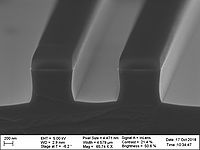
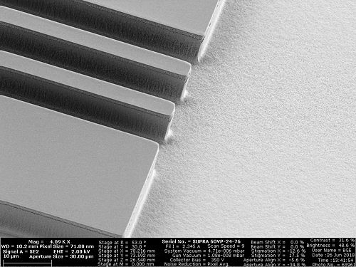
- Result of InP etching. David Larsson, DTU Photonics, 2011
-
-


InP etching June 2018
Done by Kabi and Bghe @nanolab
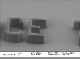
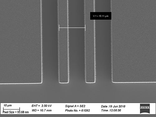
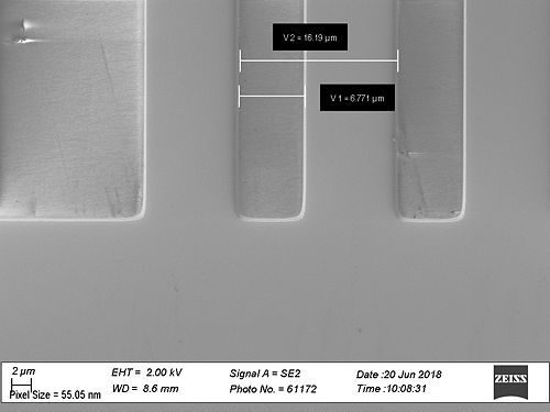
Sample pattern before etching
- Oxide mask before etching.
-
 Top view of the SiO2 mask before etching
 -
 Top view of the SiO2 mask before etching


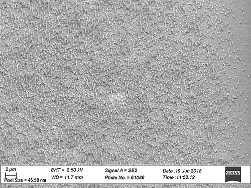
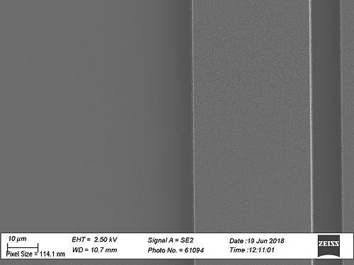
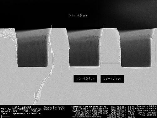
Etching of an InP piece on Si carrier
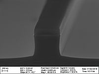
InP piece patterned with SiO2. The piece was etched on top of a Si wafer without bonding. The recipe "InP etch" was used. The roughness looks high in the bottom of the etched areas, especially in the large open areas.
- Result of InP etching.
-
 low roughness in narrow trenched
 -
 low roughness in narrow trenched
 -
 A little higher roughnedd is larger trences
 -
 Much larger roughness in open areas
 -
 Zoom in on the large roughness
 -
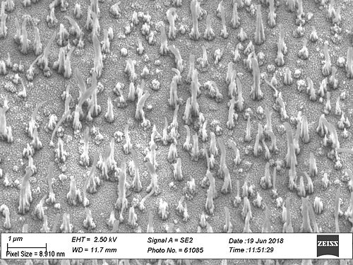 closed look at the large roughness in the open areas.


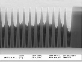
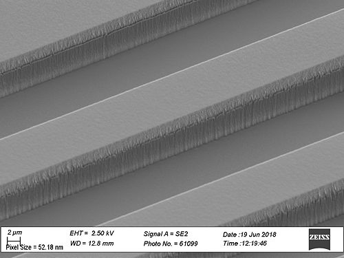
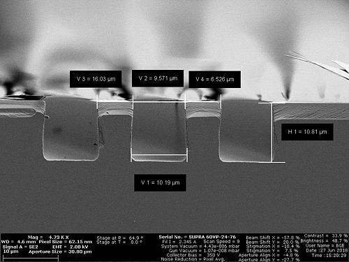
Etching of an InP piece on SiO2 carrier
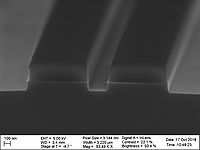
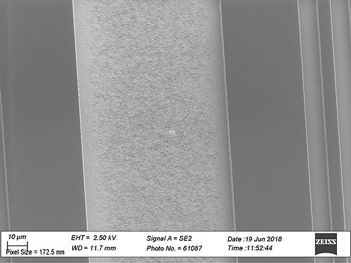
InP piece patterned with SiO2. The piece was etched on top of a Si wafer coated with SiO2 without bonding. The recipe "InP etch" was used. The roughness looks low in the bottom of the etched areas, even in the large open areas.
- Result of InP etching.
-
 Top view: oxide is gone on the narrow lines, low roughness in the trenches.
 -
 Top view: low roughness in the trenches.
 -
 30 dg view: low roughness in the trenches
 -
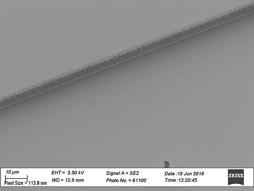 30 dg view: low roughness in the trenches
 -
 Top view: low roughness in trench and in the large area


Changing the Cl2/N2 ratio
- Result of changing the Cl2/N2 ratio.
-
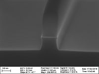
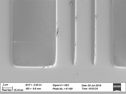
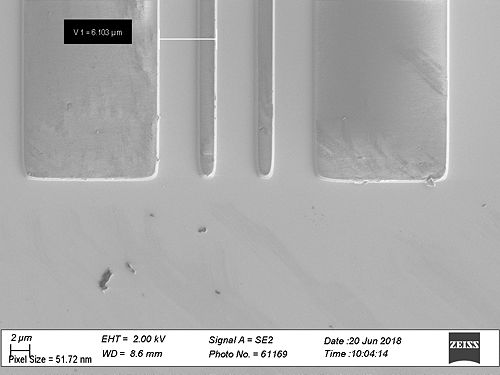
 Sample S0: Top view of the oxide mask before etching. It is the TRAVKA50 mask, but it is clear that the CD reduction is about the 1-1.5 µm of the lines.
 -
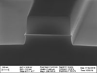
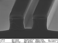
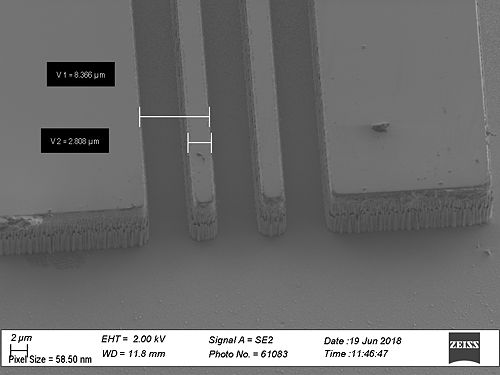
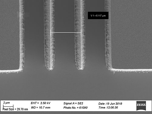
 Sample S4: Profile view. The recipe InP etch has been used.
The sample has been run on a SiO2 carrier wafer.
There is not much CD change compared to the oxide mask before the etch.
It seems like the SiO2 mask is gone and the sidewall angle from the mask has been transferred into the sample.
The sidewall profile is quit vertical in the lower part.
Etch time 15 min
Etch depth in large open areas: 9.19µm -
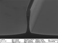
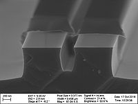
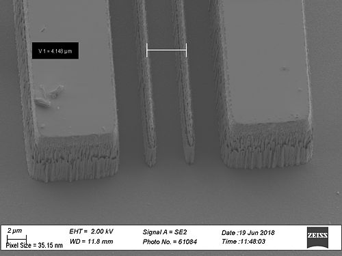
 Sample S5: Profile view. The recipe InP etch has been used but with modified Cl2 and N2 flows: N2=30 sccm Cl2=30 sccm.
The sample has been run on a SiO2 carrier wafer.
There is not much CD change compared to the oxide mask before the etch.
It seems like the SiO2 mask is gone.
The sidewall profile is overcutting probably due to too little passivation.
Etch time 10 min
Etch depth in large open areas: 11.82µm -
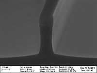
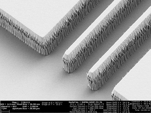 Sample S4: The sidewall roughness on the sample S4 is quite high
 -
 Sample S5: The sidewall roughness on the sample S5 is quite low.


