Specific Process Knowledge/Etch/DRIE-Pegasus/Pegasus-1: Difference between revisions
| (9 intermediate revisions by one other user not shown) | |||
| Line 3: | Line 3: | ||
[[Category: Equipment |Etch DRIE]] | [[Category: Equipment |Etch DRIE]] | ||
[[Category: Etch (Dry) Equipment|DRIE]] | [[Category: Etch (Dry) Equipment|DRIE]] | ||
{{contentbydryetch}} | |||
<!--Checked for updates on 28/6-2023 - ok/jmli --> | |||
= DRIE-Pegasus 1= | = DRIE-Pegasus 1= | ||
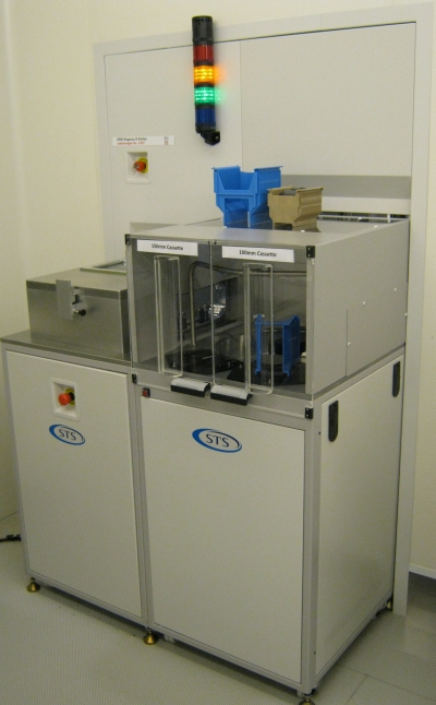
[[Image:DRIE-Pegasus.jpg |frame|left|x300px|The DRIE-Pegasus 1 load lock and cassette loader in the Nanolab cleanroom A-1]] | [[Image:DRIE-Pegasus.jpg |frame|left|x300px|The DRIE-Pegasus 1 load lock and cassette loader in the Nanolab cleanroom A-1. {{photo1}} ]] | ||
'''The user manual(s), quality control procedure(s) and results, user APV(s), technical information and contact information can be found in LabManager:''' | '''The user manual(s), quality control procedure(s) and results, user APV(s), technical information and contact information can be found in LabManager:''' | ||
| Line 48: | Line 52: | ||
*[[Specific Process Knowledge/Etch/DRIE-Pegasus/Isotropic|Isotropic etches]] | *[[Specific Process Knowledge/Etch/DRIE-Pegasus/Isotropic|Isotropic etches]] | ||
More processes, such as for DUV resist, are currently being developed, but they are not quite 'ready for publication' at LabAdviser so please contact Jonas (mailto:jmli@dtu.dk) for more information. | More processes, such as for DUV resist, are currently being developed, but they are not quite 'ready for publication' at LabAdviser so please contact Jonas ([mailto:jmli@dtu.dk jmli@dtu.dk]) for more information. | ||
<!-- *[[Specific Process Knowledge/Etch/DRIE-Pegasus/slopedsidewalls|Etches that produce positively sloped sidewalls for imprinting purposes]] --> | <!-- *[[Specific Process Knowledge/Etch/DRIE-Pegasus/slopedsidewalls|Etches that produce positively sloped sidewalls for imprinting purposes]] --> | ||
| Line 57: | Line 61: | ||
=== Advanced Processing - Henri Jansen style === | === Advanced Processing - Henri Jansen style === | ||
* [[Specific Process Knowledge/Etch/DRIE-Pegasus/Etch silicon nanostructures|Etch silicon nanostructures ]] | * [[Specific Process Knowledge/Etch/DRIE-Pegasus/Etch silicon nanostructures|Etch silicon nanostructures ]] | ||
* [[Specific Process Knowledge/Etch/DRIE-Pegasus/Etch high aspect ratio silicon microstructures|Etch high aspect ratio silicon microstructures ]] | * [[Specific Process Knowledge/Etch/DRIE-Pegasus/Etch high aspect ratio silicon microstructures|Etch high aspect ratio silicon microstructures ]] | ||
| Line 67: | Line 72: | ||
To find information on how to bond wafers or chips to a carrier wafer, click [[Specific Process Knowledge/Etch/DryEtchProcessing/Bonding| here]]. | To find information on how to bond wafers or chips to a carrier wafer, click [[Specific Process Knowledge/Etch/DryEtchProcessing/Bonding| here]]. | ||
'''Characterisation of etched trenches''' | '''Characterisation of etched trenches''' | ||
| Line 79: | Line 81: | ||
Process log at Nanolab [http://labintra.nanolab.dtu.dk/index.php/Main_Page/Process_Logs/jmli/Pegasus] | Process log at Nanolab [http://labintra.nanolab.dtu.dk/index.php/Main_Page/Process_Logs/jmli/Pegasus] | ||
Latest revision as of 09:31, 3 June 2025
Feedback to this page: click here
Unless otherwise stated, the content of this page was created by the dry etch group at DTU Nanolab
DRIE-Pegasus 1

The user manual(s), quality control procedure(s) and results, user APV(s), technical information and contact information can be found in LabManager:
Equipment info in LabManager
Process information
Hardware changes
A few hardware modifications have been made on the Pegasus since it was installed in 2010. The changes are listed below.
Other etch processes
More processes, such as for DUV resist, are currently being developed, but they are not quite 'ready for publication' at LabAdviser so please contact Jonas (jmli@dtu.dk) for more information.
Advanced Processing - Henri Jansen style
- Etch silicon nanostructures
- Etch high aspect ratio silicon microstructures
- Etch 3 dimensional silicon microstructures
- Etch black silicon
- Using OES to monitor etch process
Wafer bonding
To find information on how to bond wafers or chips to a carrier wafer, click here.
Characterisation of etched trenches
Comparing differences in etched trenches requires a set of common parameters for each trench. Click HERE to find more information about the parameters used on the DRIE-Pegasus process development.
Internal Nanolab Process log for Pegasus 1
Process log at Nanolab [1]
