Specific Process Knowledge/Thin film deposition/Electroplating-Ni: Difference between revisions
No edit summary |
|||
| (9 intermediate revisions by 3 users not shown) | |||
| Line 1: | Line 1: | ||
''' | '''<p style="color:red;">The Electroplater Technotrans microform.200 has been decomissioned. For electroplating, please contact DTU Mechanical Engineering.</p>''' | ||
[[Category: Equipment|Thin film Electroplating Ni]] | [[Category: Equipment|Thin film Electroplating Ni]] | ||
[[Category: Thin Film Deposition|Electroplating Ni]] | [[Category: Thin Film Deposition|Electroplating Ni]] | ||
= Technotrans microform.200= | |||
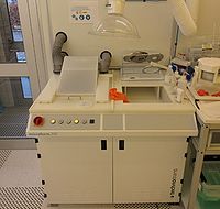
[[image:Electroplater-D3.jpg|200x200px|right|thumb|Electroplating-Ni positioned in cleanroom D-3]] | [[image:Electroplater-D3.jpg|200x200px|right|thumb|Electroplating-Ni positioned in cleanroom D-3]] | ||
| Line 29: | Line 26: | ||
Uniformity across a 4" wafer is around 5% for the standard processes (the edge being slightly thicker than the center of the sample). Running at high current densities will deposit a nickel layer that is quite soft. Decreasing current density will increase tensile strength of the deposited nickel. | Uniformity across a 4" wafer is around 5% for the standard processes (the edge being slightly thicker than the center of the sample). Running at high current densities will deposit a nickel layer that is quite soft. Decreasing current density will increase tensile strength of the deposited nickel. | ||
==Equipment performance and process related parameters== | ==Equipment performance and process related parameters== | ||
| Line 130: | Line 115: | ||
|- | |- | ||
|} | |} | ||
== DTU Nanolab Standard Programs for Electroplating of Nickel == | |||
Three different standard programs have been made by DTU Nanolab. They have all been made to fabricate nickel shims for use in the polymer injection molding machine at DTU Nanolab. For this purpose a nickel thickness of around 340-360 µm is optimal. By experimentation it has been found that the required charge for this sample thickness is 18,3 Ah. The only difference between the different standard programs is the time required for depositing the nickel. The three different standard programs deposit the ~350 µm of nickel in about 4, 6 or 12 hours respectively. | |||
The following figure shows the current profile during the first 2 hours of the programs: | |||
[[Image:CurrentProfiles2019.png|center|Current profiles of standard programs]] | |||
As can be seen from the illustration the first 30 minutes of all standard processes are identical. All processes use a slow ramping of the current. This is to make sure that some material is deposited which can conduct a higher current. Starting a plating process at several amperes is very likely to damage the sample (and possibly the sample holder) because the seed metal layer (usually 50-120 nm thick) cannot support such high currents. | |||
The Standard programs are named using the following convention: '''DCHimmXX.X-YY''' where '''DCH''' indicates it's a process developed by Nanolab, '''imm''' that is a process developed for producing samples for the '''i'''njection '''m'''olding '''m'''achine, '''XX.X''' denotes the charge in Ah (Ampere-hours) and '''YY''' denotes the approximate process time in hours. | |||
<br clear="all" /> | |||
==Comparison of standard processes== | |||
{|border="1" cellspacing="1" cellpadding="3" style="text-align:left;" | |||
|- | |||
|- | |||
|-style="background:silver; color:black" | |||
! | |||
!DCHimm18.3-04 | |||
!DCHimm18.3-06 | |||
!DCHimm18.3-12 | |||
|- | |||
|- | |||
|-style="background:WhiteSmoke; color:black" | |||
!Charge [Ah] | |||
|18,3 | |||
|18,3 | |||
|18,3 | |||
|- | |||
|- | |||
|-style="background:WhiteSmoke; color:black" | |||
!Expected nickel thickness | |||
|350 µm | |||
|350 µm | |||
|350 µm | |||
|- | |||
|- | |||
|-style="background:LightGrey; color:black" | |||
!Maximum current [A] | |||
| | |||
5,5 | |||
| | |||
3,5 | |||
| | |||
1,5 | |||
|- | |||
|- | |||
|-style="background:WhiteSmoke; color:black" | |||
!Process time [hh:mm:ss] | |||
| | |||
04:10:55 | |||
| | |||
06:12:52 | |||
| | |||
12:28:01 | |||
|- | |||
|- | |||
|-style="background:LightGrey; color:black" | |||
!Process comments | |||
| | |||
A fast program that allows one to produce two samples in a normal working day. Usually works fine for rapid prototyping. | |||
| | |||
A compromise between desired material properties (hardness, ductility, roughness) and process time. Will result in a sample that will be useful for most standard injection molding processes. | |||
| | |||
A slower process that in return results in lower roughness and stronger mechanical properties. A good choice for shims that will be used with 'harsh' injection molding parameters (high temperatures and high pressures). | |||
|- | |||
|} | |||
<br clear="all" /> | |||
Latest revision as of 15:57, 20 June 2025
The Electroplater Technotrans microform.200 has been decomissioned. For electroplating, please contact DTU Mechanical Engineering.
Technotrans microform.200

The Technotrans microform.200 (Electroplating-Ni in LabManager) is a machine capable of depositing nickel electrochemically. This is done by lowering the sample into an electrolyte containing nickel ions and then apply a voltage across the sample and the anode. The anode is a titanium basket filled with nickel pellets. The cathode is the sample to be coated with nickel.
At the anode metallic nickel is oxidized to nickel ions:
Ni (s) ⇒ Ni2+ (aq) + 2 e-
At the cathode (the sample surface), nickel ions from solution are reduced to metallic nickel:
Ni2+ (aq) + 2 e- ⇒ Ni (s)
The minimal charge accepted by the software on the machine is 0.1 Ah (Ampere-hours). This corresponds to roughly 2 µm of nickel on a four inch wafer. You can abort a program prematurely to achieve even lower thicknesses, but this requires manual control of the machine.
The maximum allowed thickness is ~1,4 mm (1400 µm), since a higher thickness will make the release of the sample difficult and likely damage the sample holder. This corresponds to a charge of 53-54 Ah on a four inch wafer. Please contact Nanolab before processing your wafer if you intend to deposit more than ~500 µm of nickel, since this can involve special challenges regarding uniformity, roughness and sample release after plating.
The plating bath is an aqueous solution of nickel sulfamate, boric acid and sulfamic acid. The bath is moderately acidic (pH = 3,70). The pH is kept constant by an automatic pH measurement and sulfamic acid dosing module. The temperature of the bath is 52°C. The sample will spin at 60 RPM during deposition.
Uniformity across a 4" wafer is around 5% for the standard processes (the edge being slightly thicker than the center of the sample). Running at high current densities will deposit a nickel layer that is quite soft. Decreasing current density will increase tensile strength of the deposited nickel.
| Parameter | Value | |
|---|---|---|
| Sample dimensions | Diameter |
50, 100 or 150 mm (~ 2", 4" or 6") |
| Sample thickness |
Maximum 1,0 mm | |
| Process parameters | Temperature |
52°C |
| pH |
3,5 - 3,8 (Recommended by manufacturer) | |
| Sample requirements | Seed metal |
Most commonly ~85-100 nm of NiV |
| Allowed materials |
Most materials allowed. See below. | |
| Forbidden materials |
Copper, cobalt. See machine manual on LabManager for details | |
| Equipment | Electroplating-Ni | |
|---|---|---|
| Purpose |
Electrochemical deposition of nickel | |
| Performance | Thickness |
~20 - 1000 µm |
| Uniformity |
Around 2-10% (depending on sample and process) | |
| Process parameter range | Temperature |
52°C |
| pH |
~3,65 (maintained automatically) | |
| Substrates | Batch size |
|
| Allowed materials |
| |
DTU Nanolab Standard Programs for Electroplating of Nickel
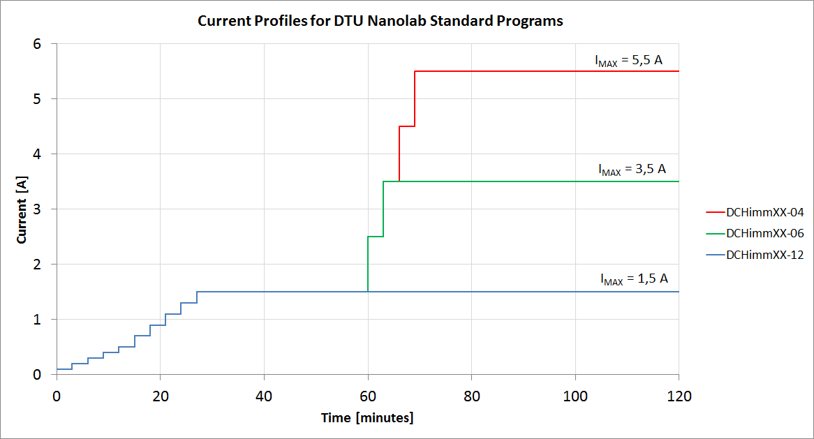
Three different standard programs have been made by DTU Nanolab. They have all been made to fabricate nickel shims for use in the polymer injection molding machine at DTU Nanolab. For this purpose a nickel thickness of around 340-360 µm is optimal. By experimentation it has been found that the required charge for this sample thickness is 18,3 Ah. The only difference between the different standard programs is the time required for depositing the nickel. The three different standard programs deposit the ~350 µm of nickel in about 4, 6 or 12 hours respectively.
The following figure shows the current profile during the first 2 hours of the programs:

As can be seen from the illustration the first 30 minutes of all standard processes are identical. All processes use a slow ramping of the current. This is to make sure that some material is deposited which can conduct a higher current. Starting a plating process at several amperes is very likely to damage the sample (and possibly the sample holder) because the seed metal layer (usually 50-120 nm thick) cannot support such high currents.
The Standard programs are named using the following convention: DCHimmXX.X-YY where DCH indicates it's a process developed by Nanolab, imm that is a process developed for producing samples for the injection molding machine, XX.X denotes the charge in Ah (Ampere-hours) and YY denotes the approximate process time in hours.
Comparison of standard processes
| DCHimm18.3-04 | DCHimm18.3-06 | DCHimm18.3-12 | |
|---|---|---|---|
| Charge [Ah] | 18,3 | 18,3 | 18,3 |
| Expected nickel thickness | 350 µm | 350 µm | 350 µm |
| Maximum current [A] |
5,5 |
3,5 |
1,5 |
| Process time [hh:mm:ss] |
04:10:55 |
06:12:52 |
12:28:01 |
| Process comments |
A fast program that allows one to produce two samples in a normal working day. Usually works fine for rapid prototyping. |
A compromise between desired material properties (hardness, ductility, roughness) and process time. Will result in a sample that will be useful for most standard injection molding processes. |
A slower process that in return results in lower roughness and stronger mechanical properties. A good choice for shims that will be used with 'harsh' injection molding parameters (high temperatures and high pressures). |
