Specific Process Knowledge/Thin film deposition/Cluster-based multi-chamber high vacuum sputtering deposition system: Difference between revisions
| (46 intermediate revisions by 4 users not shown) | |||
| Line 1: | Line 1: | ||
'''Feedback to this page''': '''[mailto: | '''Feedback to this page''': '''[mailto:labadviser@nanolab.dtu.dk?Subject=Feed%20back%20from%20page%20http://labadviser.nanolab.dtu.dk/index.php/Specific_Process_Knowledge/Thin_film_deposition/Cluster-based_multi-chamber_high_vacuum_sputtering_deposition click here]''' | ||
<i> Unless otherwise stated, this page is written by <b>DTU Nanolab internal</b><br> | |||
All images and photos on this page belonges to <b>DTU Nanolab</b></i>.<br> | |||
[[Category: Equipment|Thin film Sputter deposition Lesker]] | [[Category: Equipment|Thin film Sputter deposition Lesker]] | ||
| Line 6: | Line 11: | ||
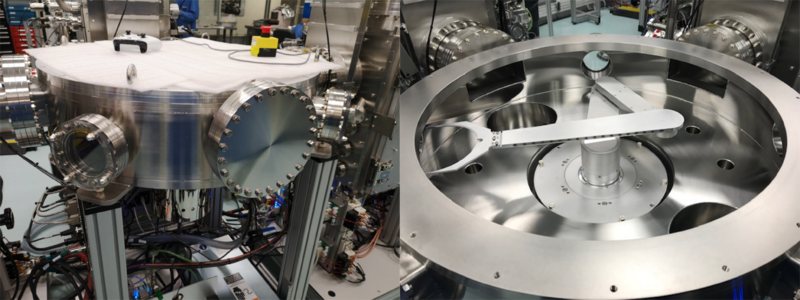
[[image:Kaempe_Lesker_image_front_page1.jpg|450x450px|right|thumb|Cluster-based multi-chamber high vacuum sputtering deposition system. View from service room Ax-1.]] | [[image:Kaempe_Lesker_image_front_page1.jpg|450x450px|right|thumb|Cluster-based multi-chamber high vacuum sputtering deposition system. View from service room Ax-1.]] | ||
The cluster-based multi-chamber high-vacuum sputtering deposition system is a robotic cluster tool with two deposition chambers sharing the same distribution transfer station and load-lock. The equipment was installed and accepted in the clean room in January 2020. The purpose of the tool is to deposit a variety of materials using DC/RF/Pulse DC/HIPIMS magnetron sputtering, with or without RF substrate bias. | |||
In <b>PC 1</b> (process chamber 1), it is possible to deposit any material using 6 x 3” magnetron sources with N<sub>2</sub> or O<sub>2</sub> reactive gases. | |||
<b>PC 3</b> (process chamber 3) is dedicated to oxygen-free materials - nitrides and metals. It is equipped with 1 x 4” + 2 x 3” magnetrons and supplied with N<sub>2</sub> process gas for reactive deposition. Both chambers allow heating of substrates up to 600 <sup>o</sup>C. The equipment is located in Cleanroom A-5, where users can access the cassette loader. | |||
| Line 15: | Line 24: | ||
'''The user manual, user APV and contact information can be found in LabManager:''' | '''The user manual, user APV, and contact information can be found in LabManager:''' | ||
<!-- remember to remove the type of documents that are not present --> | <!-- remember to remove the type of documents that are not present --> | ||
| Line 24: | Line 33: | ||
Thin Film group thinfilm@nanolab.dtu.dk is responsible | The Thin Film group <i><u>thinfilm@nanolab.dtu.dk</u></i> is responsible for the equipment. | ||
Target/Metal requests should be sent to metal@nanolab.dtu.dk | Target/Metal requests should be sent to <i><u>metal@nanolab.dtu.dk</u></i>. | ||
If you need | If you need training on the machine, please send your request to: <i><u>training@nanolab.dtu.dk</u></i>. | ||
= Sputtering deposition system set-up= | = Sputtering deposition system set-up= | ||
The cluster sputter system is used for | The cluster sputter system is used for depositing metals, magnetic metals, and dielectrics on a single 4" or 6" wafer or multiple small samples. Samples will be placed on the ten-shelf cassette and loaded in the load lock module. After the load lock chamber is pumped down, the sample can be transferred to the desired process chamber. The sample will be rotated over the target and can be heated to up to 600 °C while the film is being deposited. The system is equipped with two process chambers connected to a wafer transfer robot and a load lock chamber. | ||
<gallery caption="System set-up and power supply configuration." widths="1000px" heights="600px" perrow="1"> | <gallery caption="System set-up and power supply configuration." widths="1000px" heights="600px" perrow="1"> | ||
| Line 39: | Line 48: | ||
</gallery> | </gallery> | ||
==Power | ==Power supply configuration== | ||
Power | Power supply specifications are presented in a table below. | ||
{| border="2" cellspacing="0" cellpadding="9" | {| border="2" cellspacing="0" cellpadding="9" | ||
| Line 168: | Line 177: | ||
<b>Output Peak Current:</b> <br> | <b>Output Peak Current:</b> <br> | ||
200A nominal, <br> | 200A nominal, <br> | ||
400A | 400A tolerance | ||
| Line 206: | Line 215: | ||
== Sputter-System Metal-Oxide (PC1) == | == Sputter-System Metal-Oxide (PC1) == | ||
Chamber PC1 consists of six KJLC Torus® 3" magnetron sputtering sources with possibility of RF, DC, Pulse DC and HIPIMS sputtering. There are Argon, Nitrogen and Oxygen gas lines connected to this chamber. | Chamber PC1 consists of six KJLC Torus® 3" magnetron sputtering sources with the possibility of RF, DC, Pulse DC, and HIPIMS sputtering. There are Argon, Nitrogen, and Oxygen gas lines connected to this chamber. It is possible to apply an RF bias to the substrate, which can be used for substrate cleaning before deposition or during deposition to alter the film properties. Deposition of magnetic materials requires a high-strength magnet (HSM), which must be installed on source 3 in PC1. The chamber allows co-sputtering (sputtering from two or more sources simultaneously) as long as the sources are not connected to the same power supply. | ||
<gallery caption="Process chamber (PC 1)" widths=" | <gallery caption="Process chamber (PC 1)" widths="400px" heights="350px" perrow="2"> | ||
image:PC1_photo.png| | image:PC1_photo.png| Photo of the chamber. | ||
image:PC1_during_sputtering.png| Deposition from source 2. | image:PC1_during_sputtering.png| Deposition from source 2. | ||
</gallery> | </gallery> | ||
| Line 216: | Line 225: | ||
== Sputter-System Metal-Nitride (PC3) == | == Sputter-System Metal-Nitride (PC3) == | ||
The second process chamber | The second process chamber, designated as PC3, comprises two KJLC Torus 3" magnetron sputtering sources and one height-adjustable KJLC Torus 4" magnetron sputtering source, which also supports RF, DC, Pulse DC, and HiPIMS sputtering modes. It is possible to apply an RF bias to the substrate, which can be used to clean the substrate before deposition or during deposition to alter the film properties. The chamber allows co-sputtering (sputtering from two or more sources simultaneously) as long as the sources are not connected to the same power supply. A residual gas analyzer (RGA) mounted on the chamber allows monitoring post-process chemical gas traces. To operate the analyzer, the chamber must be pumped to its base pressure. | ||
<gallery caption="Process chamber PC 3" widths=" | <gallery caption="Process chamber PC 3" widths="400px" heights="350px" perrow="2"> | ||
image:PC3_photo.png| | image:PC3_photo.png| Photo of the chamber. | ||
image:PC3_during_sputtering.png| Deposition from source 2. | image:PC3_during_sputtering.png| Deposition from source 2. | ||
</gallery> | </gallery> | ||
| Line 225: | Line 234: | ||
==Distribution Chamber (Genmark robot)== | ==Distribution Chamber (Genmark robot)== | ||
The load-lock and process chambers PC1 and PC3 are | The load-lock and process chambers, PC1 and PC3, are connected through a standard distribution chamber. The robot arm can transfer the sample to the selected destination. During normal operation, the chamber is pumped to a base pressure, ensuring the safe transfer of the sample between chambers and the load lock without breaking the vacuum. The unit is connected to its turbo-pump. | ||
<gallery caption="Distribution chamber (Robot). View from the service area." widths="800px" heights="300px" perrow="2"> | <gallery caption="Distribution chamber (Robot). View from the service area." widths="800px" heights="300px" perrow="2"> | ||
image:arm_robot_distribution_chamber.png| The | image:arm_robot_distribution_chamber.png| The distribution chamber with and without the top cover. | ||
</gallery> | </gallery> | ||
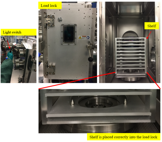
==Load-lock== | ==Load-lock== | ||
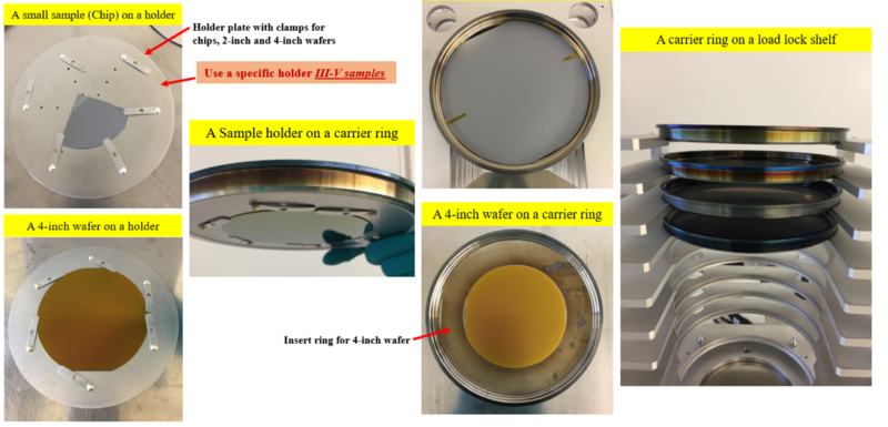
The load lock chamber is the only part of the tool that users can access. Ventilation and pumping take approximately 5 minutes. The chamber has its turbo pump. Inside, there is a shelf with 10 cassette slots. The images below show the load lock set-up and sample mounting. The shelf is designed to handle 6-inch wafers, which have to be placed on dedicated carrier rings. The rings with wafers can be introduced onto the cassette shelf. Different adapters can be used for 4-inch wafers and small chips. After the load lock is pumped, it takes approximately. It takes 6 minutes to transfer the sample into the process chamber and 8 minutes to return. | |||
<gallery caption=" | <gallery caption="Cassette loader and sample mounling." widths="800px" heights="600px" | ||
00px" perrow=" | 00px" perrow="1"> | ||
image:Kaempe_Lesker_Load_Loak_image1.png| | image:Kaempe_Lesker_Load_Loak_image1.png| The load lock chamber. | ||
image:Kaempe_Lesker_Load_Loak_image2.png| | image:Kaempe_Lesker_Load_Loak_image2.png| Sample holder, carrier ring and load lock shelf. | ||
</gallery> | </gallery> | ||
<b>Attention!</b> The shelf turns to the opposite side from where the carrier ring is loaded. Furthermore, the shelf has to be placed properly inside the load lock. A carrier ring without a sample must never be loaded in the load lock. The light in the load lock chamber can be turned on. The light switch is located on the left side of the load-lock. Process chambers PC1 and PC3 are also equipped with light switches. | |||
=Process information= | =Process information= | ||
Excessive sputter power can cause damage to the target or sputter gun. Given the target/interface thermal limitations, such damage can be reduced/eliminated by using an appropriate maximum power. However, "appropriate" often equates to "low," and a low power setting means a low deposition rate. Once the appropriate power has been established for a given target/gun, never switch it on and immediately increase the power to that value. Always increase power slowly to its maximum value through a series of ramps. When the deposition run is complete, it is equally essential to ramp down power at the same rate as it was ramped up, allowing the target to cool slowly and avoid thermal shock and the potential for target fracture. | |||
The table below shows the maximum power and maximum ramp-up/down power for available materials: | |||
{| border="2" cellspacing="0" cellpadding="9" | {| border="2" cellspacing="0" cellpadding="9" | ||
| Line 275: | Line 284: | ||
|- | |- | ||
!style="background:LightGrey; color:black" align="center" valign="center"|Au | !style="background:LightGrey; color:black" align="center" valign="center"|Au (Bonded) | ||
|style="background:WhiteSmoke; color:black" align="center"| | |style="background:WhiteSmoke; color:black" align="center"|20 | ||
|style="background:WhiteSmoke; color:black" align="center"| | |style="background:WhiteSmoke; color:black" align="center"|140 | ||
|style="background:WhiteSmoke; color:black" align="center"| | |style="background:WhiteSmoke; color:black" align="center"|0.3 | ||
|style="background:WhiteSmoke; color:black" align="center"|DC/HiPIMS | |style="background:WhiteSmoke; color:black" align="center"|DC/HiPIMS | ||
| Line 316: | Line 325: | ||
|style="background:WhiteSmoke; color:black" align="center"|10 | |style="background:WhiteSmoke; color:black" align="center"|10 | ||
|style="background:WhiteSmoke; color:black" align="center"|High | |style="background:WhiteSmoke; color:black" align="center"|High Strengh Magnets /DC | ||
|- | |- | ||
| Line 373: | Line 382: | ||
|style="background:WhiteSmoke; color:black" align="center"|0.3 | |style="background:WhiteSmoke; color:black" align="center"|0.3 | ||
|style="background:WhiteSmoke; color:black" align="center"| | |style="background:WhiteSmoke; color:black" align="center"|PDC | ||
| Line 417: | Line 426: | ||
Additional information about the processes and equipment performace can be found here: | |||
*Pre-acceptance test [[:File:Cluster-based multi-chamber high vacuum sputtering deposition system pre acceptance.pptx]] | |||
*Acceptance test [[:File:Cluster Lesker P1 and P3 Acceptance test FOR LA PUBLICATION.pdf]] | |||
==Maximum Power Calculation== | |||
* <math>PD</math> - Power density (fundamental constant given by a supplier) | |||
* <math>P(W)</math> - Power (W) from power supply | |||
* <math>A(inch^2)</math> - Area of the target | |||
------------------------------------------------------------------------------------------------------------ | |||
<math> PD=\frac{P(W)}{A(inch^2)}</math> ⇒ <math>P(W)=PD\cdot A(inch^2)=PD\cdot\frac{\pi d^2}{4}</math> | |||
<ul> | |||
<li><p> <b><span style="color: green">d=2" (2-inch target)</span></b> <math>P(W)=3.14\cdot PD</math> </p></li> | |||
<li><p> <b><span style="color: green">d=3" (3-inch target)</span></b> <math>P(W)=7.065\cdot PD</math> </p></li> | |||
<li><p> <b><span style="color: green">d=4" (4-inch target)</span></b> <math>P(W)=12.56\cdot PD</math> </p></li> | |||
<li><p> <b><span style="color: green">d=6" (6-inch target)</span></b> <math>P(W)=28.26\cdot PD</math> </p></li> | |||
</ul> | |||
-------------------------------------------------- | |||
Value of the <math>PD</math> is material dependent and can be found on KJLC homepage | |||
| Line 431: | Line 460: | ||
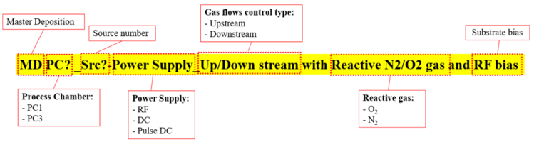
There are | There are 76 developed and tested process recipes for general users (48 for PC1 and 28 for PC3). They include non-reactive and reactive DC, RF, and PulseDC sputtering with or without substrate bias. Deposition using HiPIMS can only be performed with the assistance of DTU Nanolab staff. Starting the recipe, the user can adjust the relevant process parameters, including power, pressure, reactive gas ratio, rotation speed, substrate bias, and others. Each of the 76 recipes has a unique name which indicates the process chamber, type of sputtering (DC, RF, or Pulse DC), gas flow control, the type of reactive gas, and the presence of substrate bias. In addition to the standard process recipes, there are also recipes for substrate heating and RF cleaning. | ||
<gallery caption=" | <gallery caption="The build-up of the standard recipe name" widths="800px" heights="200px" perrow="1"> | ||
image:Kaempe_Lesker_standard_recipe_name.png| Deposition | image:Kaempe_Lesker_standard_recipe_name.png| The standard recipe has its unique name starting with the letters "MD", which stands for "Master Deposition". | ||
</gallery> | </gallery> | ||
So far, the following results can be used as a guide or reference: | |||
(Look for updated information in a specific [[Specific_Process_Knowledge/Thin_film_deposition|material list]]). | |||
| Line 610: | Line 640: | ||
|} | |} | ||
<br> | |||
<!------> | |||
<br> | |||
==Substrate heating== | |||
There are software interlocks that | During the test by KJLC, using a wafer with thermocouples attached, the temperature of the wafer and the control thermocouple could be monitored. Generally, the sample temperature will be approximately 50 degrees lower than the temperature displayed on the system. There are software interlocks that control/protect the heater, as well as a hardware interlock that prevents the heater from turning on when the chamber is at atmospheric pressure or if there is insufficient water flow in the system. | ||
There is | There are software interlocks that prevent the transfer port from opening while the heater is on. Additionally, it will not allow the heater to turn on if there is no assigned wafer in the chamber, and it will not open the chamber vent valve if the temperature exceeds 80 °C. | ||
There is no sensor to detect if a sample is physically present. If a user transfers an empty wafer carrier into a process chamber, the wafer ID will update accordingly, and the heater can be activated. | |||
A sample transfer can be done while the sample is hot, but not while the heater is on. The heater thermocouples will cool very rapidly as soon as the heater is turned off, so there is no set temperature. A sample transfer unload should be done when the temperature is below 300 °C. | |||
There are dedicated recipes to turn on a heater: | There are dedicated recipes to turn on a heater: | ||
| Line 635: | Line 667: | ||
==Substrate cleaning (RF Bias)== | ==Substrate cleaning (RF Bias)== | ||
RF cleaning can be used to clean the sample before the deposition. There are dedicated recipes for that: | |||
* If PC1 is used, select “Master Bias PC1_Upstream” | * If PC1 is used, select “Master Bias PC1_Upstream” | ||
| Line 641: | Line 673: | ||
* If PC3 is used, select “Master Bias PC3_Upstream” | * If PC3 is used, select “Master Bias PC3_Upstream” | ||
The user can select rotation speed (10 rpm), process pressure (1-15mTorr) RF power (maximum 100 W) and cleaning time (maximum 1800 s). | The user can select rotation speed (10 rpm), process pressure (1-15mTorr), RF power (maximum 100 W), and cleaning time (maximum 1800 s). | ||
==Batch process== | ==Batch process== | ||
The advanced system with the cassette loader and robot arm allow running a batch process ("Master Cassette" recipes). These processes are not among the standard recipes but can be developed by DTU Nanolab upon request. | |||
Latest revision as of 15:43, 30 July 2025
Feedback to this page: click here
Unless otherwise stated, this page is written by DTU Nanolab internal
All images and photos on this page belonges to DTU Nanolab.

The cluster-based multi-chamber high-vacuum sputtering deposition system is a robotic cluster tool with two deposition chambers sharing the same distribution transfer station and load-lock. The equipment was installed and accepted in the clean room in January 2020. The purpose of the tool is to deposit a variety of materials using DC/RF/Pulse DC/HIPIMS magnetron sputtering, with or without RF substrate bias.
In PC 1 (process chamber 1), it is possible to deposit any material using 6 x 3” magnetron sources with N2 or O2 reactive gases.
PC 3 (process chamber 3) is dedicated to oxygen-free materials - nitrides and metals. It is equipped with 1 x 4” + 2 x 3” magnetrons and supplied with N2 process gas for reactive deposition. Both chambers allow heating of substrates up to 600 oC. The equipment is located in Cleanroom A-5, where users can access the cassette loader.
Manufacture: Kurt J. Lesker Company
Model: 2017 PRO Line PVD75 thin film deposition cluster system
The user manual, user APV, and contact information can be found in LabManager:
Sputter-System Metal-Oxide(PC1)
Sputter-System Metal-Nitride(PC3)
The Thin Film group thinfilm@nanolab.dtu.dk is responsible for the equipment.
Target/Metal requests should be sent to metal@nanolab.dtu.dk.
If you need training on the machine, please send your request to: training@nanolab.dtu.dk.
Sputtering deposition system set-up
The cluster sputter system is used for depositing metals, magnetic metals, and dielectrics on a single 4" or 6" wafer or multiple small samples. Samples will be placed on the ten-shelf cassette and loaded in the load lock module. After the load lock chamber is pumped down, the sample can be transferred to the desired process chamber. The sample will be rotated over the target and can be heated to up to 600 °C while the film is being deposited. The system is equipped with two process chambers connected to a wafer transfer robot and a load lock chamber.
- System set-up and power supply configuration.
-
 The system set-up showing the different operation chambers and power supplies network.
*HSM - High Strengh Magnet.
**RGA - Residual Gas Analyser.

Power supply configuration
Power supply specifications are presented in a table below.
| Power Supply ID | Type | Maximum output power (W) | Maximum output voltage (V) | Maximum output current (A) | Comments
|
|---|---|---|---|---|---|
| PC1 Power Supply 1 | RF | 300 | |||
| PC1 Power Supply 3 | DC | 500 | 1000 | 4 | |
| PC1 Power Supply 4 | DC | 500 | 1000 | 4 | |
| PC1 Power Supply 5 | Pulse DC | 2000 | 800 | 5 |
Max frequency: 100kHz |
| PC1 Power Supply 7 | RF (Substrate) | 100 | |||
| PC3 Power Supply 1 | RF | 300 | |||
| PC3 Power Supply 2 | Pulse DC | 2000 | 800 | 5 |
Max frequency: 100kHz |
| PC3 Power Supply 3 | DC to HiPIMS | 1500 | 1000 | 4 |
HiPIMS Unit
|
| PC3 Power Supply 5 | DC | 500 | 1000 | 4 |
|
| PC3 Power Supply 6 | RF (substrate) | 100 |
Sputter-System Metal-Oxide (PC1)
Chamber PC1 consists of six KJLC Torus® 3" magnetron sputtering sources with the possibility of RF, DC, Pulse DC, and HIPIMS sputtering. There are Argon, Nitrogen, and Oxygen gas lines connected to this chamber. It is possible to apply an RF bias to the substrate, which can be used for substrate cleaning before deposition or during deposition to alter the film properties. Deposition of magnetic materials requires a high-strength magnet (HSM), which must be installed on source 3 in PC1. The chamber allows co-sputtering (sputtering from two or more sources simultaneously) as long as the sources are not connected to the same power supply.
- Process chamber (PC 1)
-
 Photo of the chamber.
 -
 Deposition from source 2.


Sputter-System Metal-Nitride (PC3)
The second process chamber, designated as PC3, comprises two KJLC Torus 3" magnetron sputtering sources and one height-adjustable KJLC Torus 4" magnetron sputtering source, which also supports RF, DC, Pulse DC, and HiPIMS sputtering modes. It is possible to apply an RF bias to the substrate, which can be used to clean the substrate before deposition or during deposition to alter the film properties. The chamber allows co-sputtering (sputtering from two or more sources simultaneously) as long as the sources are not connected to the same power supply. A residual gas analyzer (RGA) mounted on the chamber allows monitoring post-process chemical gas traces. To operate the analyzer, the chamber must be pumped to its base pressure.
- Process chamber PC 3
-
 Photo of the chamber.
 -
 Deposition from source 2.


Distribution Chamber (Genmark robot)
The load-lock and process chambers, PC1 and PC3, are connected through a standard distribution chamber. The robot arm can transfer the sample to the selected destination. During normal operation, the chamber is pumped to a base pressure, ensuring the safe transfer of the sample between chambers and the load lock without breaking the vacuum. The unit is connected to its turbo-pump.
- Distribution chamber (Robot). View from the service area.
-
 The distribution chamber with and without the top cover.

Load-lock
The load lock chamber is the only part of the tool that users can access. Ventilation and pumping take approximately 5 minutes. The chamber has its turbo pump. Inside, there is a shelf with 10 cassette slots. The images below show the load lock set-up and sample mounting. The shelf is designed to handle 6-inch wafers, which have to be placed on dedicated carrier rings. The rings with wafers can be introduced onto the cassette shelf. Different adapters can be used for 4-inch wafers and small chips. After the load lock is pumped, it takes approximately. It takes 6 minutes to transfer the sample into the process chamber and 8 minutes to return.
- Cassette loader and sample mounling.
-
 The load lock chamber.
 -
 Sample holder, carrier ring and load lock shelf.


Attention! The shelf turns to the opposite side from where the carrier ring is loaded. Furthermore, the shelf has to be placed properly inside the load lock. A carrier ring without a sample must never be loaded in the load lock. The light in the load lock chamber can be turned on. The light switch is located on the left side of the load-lock. Process chambers PC1 and PC3 are also equipped with light switches.
Process information
Excessive sputter power can cause damage to the target or sputter gun. Given the target/interface thermal limitations, such damage can be reduced/eliminated by using an appropriate maximum power. However, "appropriate" often equates to "low," and a low power setting means a low deposition rate. Once the appropriate power has been established for a given target/gun, never switch it on and immediately increase the power to that value. Always increase power slowly to its maximum value through a series of ramps. When the deposition run is complete, it is equally essential to ramp down power at the same rate as it was ramped up, allowing the target to cool slowly and avoid thermal shock and the potential for target fracture.
The table below shows the maximum power and maximum ramp-up/down power for available materials:
| Target size | Target material | Maximum Power density (W/inch2) | Maximum Power (W) | Maximum Ramp up/down Power (W/s) | Comments
|
|---|---|---|---|---|---|
| 3 inch | Al | 150 | 1000 | 10 | DC/HiPIMS |
| Au (Bonded) | 20 | 140 | 0.3 | DC/HiPIMS | |
| Ag | 100 | 700 | 10 | DC/HiPIMS | |
| Cu | 200 | 1400 | 10 | DC/HiPIMS | |
| Ni | 50 | 350 | 10 | High Strengh Magnets /DC | |
| Ti | 50 | 350 | 10 | DC/HiPIMS | |
| Ge (Bonded) | 20 | 140 | 0.3 | DC/RF | |
| Si (Unbonded/Bonded) | 20 | 140 | 0.3 | RF
| |
| SiO2 (Bonded) | 20 | 140 | 0.3 | RF
| |
| ITO (Bonded) | 20 | 140 | 0.3 | PDC
| |
| BaTiO3 (Bonded) | 20 | 140 | 0.3 | RF
| |
| NbTi | 50 | 350 | 10 | DC | |
| 4 inch | Al | 150 | 1800 | 10 | DC/HiPIMS |
Additional information about the processes and equipment performace can be found here:
- Pre-acceptance test File:Cluster-based multi-chamber high vacuum sputtering deposition system pre acceptance.pptx
Maximum Power Calculation
- - Power density (fundamental constant given by a supplier)
- - Power (W) from power supply
- - Area of the target
⇒
d=2" (2-inch target)
d=3" (3-inch target)
d=4" (4-inch target)
d=6" (6-inch target)
Value of the is material dependent and can be found on KJLC homepage
Standard recipe performance
There are 76 developed and tested process recipes for general users (48 for PC1 and 28 for PC3). They include non-reactive and reactive DC, RF, and PulseDC sputtering with or without substrate bias. Deposition using HiPIMS can only be performed with the assistance of DTU Nanolab staff. Starting the recipe, the user can adjust the relevant process parameters, including power, pressure, reactive gas ratio, rotation speed, substrate bias, and others. Each of the 76 recipes has a unique name which indicates the process chamber, type of sputtering (DC, RF, or Pulse DC), gas flow control, the type of reactive gas, and the presence of substrate bias. In addition to the standard process recipes, there are also recipes for substrate heating and RF cleaning.
- The build-up of the standard recipe name
-
 The standard recipe has its unique name starting with the letters "MD", which stands for "Master Deposition".

So far, the following results can be used as a guide or reference:
(Look for updated information in a specific material list).
| Recipe name | Target material | Pressure (mTorr) | Power (W) | Deposition rate (nm/min) | Uniformity (%) on 6 inch wafer |
Comments
|
|---|---|---|---|---|---|---|
| MD PC1 Src1 RF Upstream | SiO2 | 3 | 140 (RF) | 2.3 | 0.5 | |
| MD PC1 Src2 RF Upstream | SiO2 | 3 | 140 (RF) | 2.6 | 3 | |
| MD PC1 Src3 DC Upstream | Ni | 3 | 500 (DC) | 23.3 | 2.5 | |
| MD PC1 Src4 DC Upstream | Cu | 3 | 500 (DC) | 52.2 | 2.2 | |
| MD PC1 Src5 DC Upstream | Al | 3 | 200 (DC) | 7.9 | 3.2 | |
| MD PC1 Src5 Pulse DC Downstream with reactive O2 |
Al | 3 | 500 (PDC) Frequency: 100Hz Reverse time: 2µs |
1.7 | 3.4 | Ar flow: 50sccm O2 flow: 15 sccm
|
| MD PC1 Src6 Pulse DC Upstream | ITO | 3 | 140 (PDC) Frequency: 100Hz Reverse time: 2µs |
11 | 4.5 | |
| MD PC1 Src6 Pulse DC Downstream with reactive O2 |
ITO | 3 | 140 (PDC) Frequency: 100Hz Reverse time: 2µs |
11.3 | - | Ar flow: 50sccm O2 flow: 2 sccm |
| MD PC1 Src1 RF Upstream | Si | 3 | 120 (RF) | 1.8 | - | |
| MD PC3 Src1 Pulse DC Downstream with reactive N2 |
Al | 3 | 900 (PDC) Frequency: 100Hz Reverse time: 2µs |
29 | 3.2 | Ar flow: 50sccm O2 flow: 15 sccm |
Substrate heating
During the test by KJLC, using a wafer with thermocouples attached, the temperature of the wafer and the control thermocouple could be monitored. Generally, the sample temperature will be approximately 50 degrees lower than the temperature displayed on the system. There are software interlocks that control/protect the heater, as well as a hardware interlock that prevents the heater from turning on when the chamber is at atmospheric pressure or if there is insufficient water flow in the system.
There are software interlocks that prevent the transfer port from opening while the heater is on. Additionally, it will not allow the heater to turn on if there is no assigned wafer in the chamber, and it will not open the chamber vent valve if the temperature exceeds 80 °C.
There is no sensor to detect if a sample is physically present. If a user transfers an empty wafer carrier into a process chamber, the wafer ID will update accordingly, and the heater can be activated.
A sample transfer can be done while the sample is hot, but not while the heater is on. The heater thermocouples will cool very rapidly as soon as the heater is turned off, so there is no set temperature. A sample transfer unload should be done when the temperature is below 300 °C.
There are dedicated recipes to turn on a heater:
- If PC1 is used, select “Master Heater PC1 - On”
- If PC3 is used, select “Master Heater PC3 - On”
Substrate cleaning (RF Bias)
RF cleaning can be used to clean the sample before the deposition. There are dedicated recipes for that:
- If PC1 is used, select “Master Bias PC1_Upstream”
- If PC3 is used, select “Master Bias PC3_Upstream”
The user can select rotation speed (10 rpm), process pressure (1-15mTorr), RF power (maximum 100 W), and cleaning time (maximum 1800 s).
Batch process
The advanced system with the cassette loader and robot arm allow running a batch process ("Master Cassette" recipes). These processes are not among the standard recipes but can be developed by DTU Nanolab upon request.