LabAdviser/Technology Research/Nanoscale characterization of ultra-thin metal films for nanofabrication applications: Difference between revisions
mNo edit summary |
|||
| (60 intermediate revisions by 3 users not shown) | |||
| Line 1: | Line 1: | ||
'''Feedback to this page''': '''[mailto:labadviser@ | '''Feedback to this page''': '''[mailto:labadviser@nanolab.dtu.dk?Subject=Feed%20back%20from%20page%20http://labadviser.nanolab.dtu.dk/index.php/LabAdviser/Technology_Research/Nanoscale_characterization_of_ultra-thin_metal_films_for_nanofabrication_applications click here]''' | ||
=Nanoscale characterization of ultra-thin metal films for nanofabrication applications= | =Nanoscale characterization of ultra-thin metal films for nanofabrication applications= | ||
*'''Project type:''' Ph.D. project | *'''Project type:''' Ph.D. project | ||
*'''Project responsible:''' Matteo Todeschini | *'''Project responsible:''' Matteo Todeschini ([http://orbit.dtu.dk/en/persons/matteo-todeschini(06c8b80c-b670-4bc3-8547-f5dd723de085).html DTU Orbit]) | ||
*'''Supervisors''' | *'''Supervisors:''' Prof. Jakob Birkedal Wagner, Assoc. Prof. Flemming Jensen, Assist. Prof. Anpan Han | ||
*'''Partners involved:''' DTU Danchip/ | *'''Partners involved:''' DTU Nanolab (former DTU Danchip and DTU CEN) | ||
*'''Full thesis:''' [[:File:PhDthesis_opponent changes_final.pdf|Link]] | |||
*'''Overview:''' [[Specific Process Knowledge/Thin film deposition/Deposition of Gold/Adhesion layers|Adhesion layers]] | |||
*'''Overview:''' [[LabAdviser/314/Microscopy 314-307/SEM/Nova/Transmission Kikuchi diffraction|Transmission Kikuchi diffraction]] | |||
==Project Description== | ==Project Description== | ||
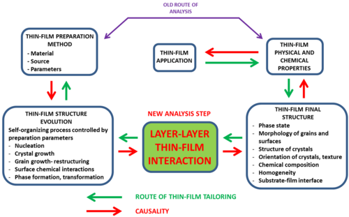
[[File:1.png|500px|thumb|Fig. 1. Schematic representation of the "thin-film structure-property causality" approach for the fabrication of thin-films. The study of the interaction between thin-films is added as fundamental step in the process.]] | |||
With the constant miniaturization of the devices and the fabrication of increasingly complex multi-material structures, the interaction between different ultra-thin layers has gained considerable importance in the field of thin-film science and technology in recent years. Therefore the characterization of such interactions in a wide range of temperatures and the description of their impact on the chemical composition, morphology and distribution of crystallographic orientations of multilayer thin-films is of utmost importance. | The deposition of metal thin-film structures on dielectric or semiconductor substrates is central for the fabrication of structures and devices having nanoscale characteristic dimension. With the constant miniaturization of the devices and the fabrication of increasingly complex multi-material structures, the interaction between different ultra-thin layers has gained considerable importance in the field of thin-film science and technology in recent years. Therefore the characterization of such interactions in a wide range of temperatures and the description of their impact on the chemical composition, morphology and distribution of crystallographic orientations of multilayer thin-films is of utmost importance. | ||
This PhD project focuses on the description of the interaction at the nanoscale level between noble metal films, widely used in different areas of micro- and nanofabrication, and extremely thin films of reactive transition metals, used to enhance adhesion onto the substrate - and thus referred as "adhesion layers". In particular, the work focused on the study of pure Au films and Cr/Au and Ti/Au bilayer and multilayer systems, which were analyzed at different temperatures using a spectrum of complementary characterization techniques. This choice has been done due to the importance and extensive use of such materials in a wide range of micro- and nanofabrication applications, including plasmonic structures for biosensing, optical antennas and single-molecule spectroscopic devices, 2D field effect and organic transistors, multilayer structures for photonic structures and | |||
metamaterials, nanopores for bio-detection, ultracompact resonators, substrates for graphene growth and devices for nanoimaging as nanolenses and waveguides. | |||
The final aim is to add a further fundamental step in the "thin-film structure-property causality" approach visible in Fig. 1. | |||
The project involved the introduction of the recently developed transmission Kikuchi diffraction (TKD) technique for the characterization of the crystal structure, grain size, and crystallographic texture of polycrystalline thin films. The remarkable potential of TKD for the in-situ analysis of thin films at elevated temperatures was revealed through the in-situ investigation of solid-state dewetting of Au, enabling to observe the start of the dewetting at a temperature as low as 150°C and demonstrating the crucial role of temperature in the modification of the nanostructure of metal thin films during nanofabrication. The data acquired during solid state dewetting were used to qualitatively study the formation and expansion of the holes in the film. A new criterion for the detection of the temperature of formation of the holes in the film was introduced and an in-situ monitoring of the formation and expansion of the holes in the Au film was also performed. This allowed to observe the formation of the holes exclusively in the positions of high surface energy grains and the reduction of the interface energy of the system by the elimination of grain boundaries and by grain coalescence. | |||
The influence that Ti and Cr adhesion layers have on the microscopic and macroscopic properties of Au ultra-thin metal films was investigated at room temperature, with the analysis carried out on both bilayer and multilayer systems in order to obtain a more complete view of the interaction. The obtained results led to the formulation of a revised adhesion model for the Ti/Au and Cr/Au bilayer systems, which gives a description of the adhesion layer-overlayer interaction and can be used by the research community as guide-lines for adhesion layer and thin-film stack engineering. The model was also accompanied by the formulation of recommendations about the use of adhesion layers for different nanofabrication applications. The analysis of Ti/Au/Ti and Cr/Au/Cr multilayer systems allowed to obtain experimental evidence of the type of chemical bonding that leads to the increase of adhesion. A positive impact of the adhesion layers on the stability of the Au nanostructure at high temperatures was observed with TKD, with Ti and Cr preserving the continuity of the Au layer up to a temperature of 500°C without the observation of dewetting. | |||
==Dissemination== | |||
===Publications in Peer Reviewed Journals=== | |||
*; Influence of Ti and Cr adhesion layers on ultrathin Au films | |||
*: [[File:1.gif|350px]] | |||
*: [https://pubs.acs.org/doi/abs/10.1021/acsami.7b10136 Link to Article] | |||
*: <u>M. Todeschini</u>, A. B. da Silva Fanta, F. Jensen, J. B. Wagner, and A. Han<br> ''ACS Appl. Mater. Interfaces'', vol. 9 (42), pp. 37374–37385, 2017. | |||
** '''Overview:''' [[Specific Process Knowledge/Thin film deposition/Deposition of Gold/Adhesion layers|Adhesion layers]] | |||
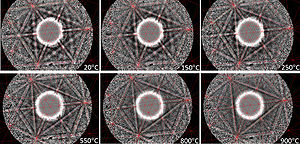
*; Elevated temperature transmission Kikuchi diffraction in the SEM | |||
*: [[File:2.jpg|300px]] | |||
*: [https://www.sciencedirect.com/science/article/pii/S1044580318300937 Link to Article] | |||
*: A. B. da Silva Fanta, <u>M. Todeschini</u>, A. Burrows, H. Jansen, C. D. Damsgaard, H. Alimadadi, and J. B. Wagner<br> ''Materials Characterization'', vol. 139, pp. 452-462, 2018. | |||
** '''Overview:''' [[LabAdviser/314/Microscopy 314-307/SEM/Nova/Transmission Kikuchi diffraction|Transmission Kikuchi diffraction]] | |||
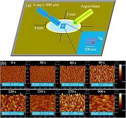
*; In-depth evolution of chemical states and sub-10-nm-resolution crystal orientation mapping of nanograins in Ti(5 nm)/Au(20 nm)/Cr(3 nm) trilayer thin films | |||
*: [[File:3.jpg|250px]] | |||
*: [https://www.sciencedirect.com/science/article/pii/S0169433218313187 Link to Article] | |||
*: X. Zhu, <u>M. Todeschini</u>, A. B. da Silva Fanta, L. Liu, F. Jensen, J. Hübner, H. Jansen, A. Han, P. Shi, A. Ming, and C. Xie<br> ''Applied Surface Science'', vol. 453, pp. 365-372, 2018. | |||
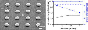
*; Inductively coupled plasma nanoetching of atomic layer deposition alumina | |||
*: [[File:Graphical Abstract2.jpg|300px]] | |||
*: [https://doi.org/10.1016/j.mee.2018.02.023 Link to Article] | |||
*: A. Han, B. Chang, <u>M. Todeschini</u>, H. T. Le, W. Tiddi and M. Keil<br> ''Microelectronic Engineering'', vol. 193, pp. 28-33, 2018. | |||
===Conferences and Workshops Contributions=== | |||
2017 | |||
*; Complementary electron microscopic-spectroscopic characterization of Ti and Cr adhesion layers | |||
*: <u>M. Todeschini</u>, A. B. da Silva Fanta, J. B. Wagner, F. Jensen, A. Han<br> Abstract and Poster at ''43rd International conference on Micro and Nano Engineering'', Braga, Portugal, 2017. | |||
*; Electron Microscopy Characterization of Adhesion Layer Influence on Ultra-thin Gold Films | |||
*: <u>M. Todeschini</u>, A. B. da Silva Fanta, F. Jensen, A. Han, J. B. Wagner<br> Oral presentaion at ''68th Annual Conference of the Nordic Microscopy Society (SCANDEM 2017)'', Reykjavík, Iceland, 2017. | |||
2016 | |||
*; Investigation with complementary characterization methods of adhesion layer effect on nanostructure of gold ultra-thin films | |||
*: <u>M. Todeschini</u>, J. B. Wagner, F. Jensen, A. Han<br> Abstract and Poster at ''42nd International conference on Micro and Nano Engineering'', Vienna, Austria, 2016. | |||
*; Atomic layer deposition instrument for in-situ environmental TEM imaging of ALD process | |||
*: <u>M. Todeschini</u>, P. Windmann, F. Jensen, J. B. Wagner, A. Han<br> Abstract and Poster at ''42nd International conference on Micro and Nano Engineering'', Vienna, Austria, 2016. | |||
*; Adhesion layer investigation with complementary characterization methods for energy loss reduction in electronic nanodevices | |||
*: <u>M. Todeschini</u>, A. B. da Silva Fanta, A. Burrows, J. B. Wagner, F. Jensen, A. Han<br> Oral presentation at ''Sustain-ATV Conference 2016'', Kgs. Lyngby, Denmark, 2016. | |||
Latest revision as of 10:59, 17 June 2025
Feedback to this page: click here
Nanoscale characterization of ultra-thin metal films for nanofabrication applications
- Project type: Ph.D. project
- Project responsible: Matteo Todeschini (DTU Orbit)
- Supervisors: Prof. Jakob Birkedal Wagner, Assoc. Prof. Flemming Jensen, Assist. Prof. Anpan Han
- Partners involved: DTU Nanolab (former DTU Danchip and DTU CEN)
- Full thesis: Link
- Overview: Adhesion layers
- Overview: Transmission Kikuchi diffraction
Project Description

The deposition of metal thin-film structures on dielectric or semiconductor substrates is central for the fabrication of structures and devices having nanoscale characteristic dimension. With the constant miniaturization of the devices and the fabrication of increasingly complex multi-material structures, the interaction between different ultra-thin layers has gained considerable importance in the field of thin-film science and technology in recent years. Therefore the characterization of such interactions in a wide range of temperatures and the description of their impact on the chemical composition, morphology and distribution of crystallographic orientations of multilayer thin-films is of utmost importance.
This PhD project focuses on the description of the interaction at the nanoscale level between noble metal films, widely used in different areas of micro- and nanofabrication, and extremely thin films of reactive transition metals, used to enhance adhesion onto the substrate - and thus referred as "adhesion layers". In particular, the work focused on the study of pure Au films and Cr/Au and Ti/Au bilayer and multilayer systems, which were analyzed at different temperatures using a spectrum of complementary characterization techniques. This choice has been done due to the importance and extensive use of such materials in a wide range of micro- and nanofabrication applications, including plasmonic structures for biosensing, optical antennas and single-molecule spectroscopic devices, 2D field effect and organic transistors, multilayer structures for photonic structures and metamaterials, nanopores for bio-detection, ultracompact resonators, substrates for graphene growth and devices for nanoimaging as nanolenses and waveguides.
The final aim is to add a further fundamental step in the "thin-film structure-property causality" approach visible in Fig. 1.
The project involved the introduction of the recently developed transmission Kikuchi diffraction (TKD) technique for the characterization of the crystal structure, grain size, and crystallographic texture of polycrystalline thin films. The remarkable potential of TKD for the in-situ analysis of thin films at elevated temperatures was revealed through the in-situ investigation of solid-state dewetting of Au, enabling to observe the start of the dewetting at a temperature as low as 150°C and demonstrating the crucial role of temperature in the modification of the nanostructure of metal thin films during nanofabrication. The data acquired during solid state dewetting were used to qualitatively study the formation and expansion of the holes in the film. A new criterion for the detection of the temperature of formation of the holes in the film was introduced and an in-situ monitoring of the formation and expansion of the holes in the Au film was also performed. This allowed to observe the formation of the holes exclusively in the positions of high surface energy grains and the reduction of the interface energy of the system by the elimination of grain boundaries and by grain coalescence.
The influence that Ti and Cr adhesion layers have on the microscopic and macroscopic properties of Au ultra-thin metal films was investigated at room temperature, with the analysis carried out on both bilayer and multilayer systems in order to obtain a more complete view of the interaction. The obtained results led to the formulation of a revised adhesion model for the Ti/Au and Cr/Au bilayer systems, which gives a description of the adhesion layer-overlayer interaction and can be used by the research community as guide-lines for adhesion layer and thin-film stack engineering. The model was also accompanied by the formulation of recommendations about the use of adhesion layers for different nanofabrication applications. The analysis of Ti/Au/Ti and Cr/Au/Cr multilayer systems allowed to obtain experimental evidence of the type of chemical bonding that leads to the increase of adhesion. A positive impact of the adhesion layers on the stability of the Au nanostructure at high temperatures was observed with TKD, with Ti and Cr preserving the continuity of the Au layer up to a temperature of 500°C without the observation of dewetting.
Dissemination
Publications in Peer Reviewed Journals
- Influence of Ti and Cr adhesion layers on ultrathin Au films

- Link to Article
- M. Todeschini, A. B. da Silva Fanta, F. Jensen, J. B. Wagner, and A. Han
ACS Appl. Mater. Interfaces, vol. 9 (42), pp. 37374–37385, 2017.
- Overview: Adhesion layers
- Elevated temperature transmission Kikuchi diffraction in the SEM

- Link to Article
- A. B. da Silva Fanta, M. Todeschini, A. Burrows, H. Jansen, C. D. Damsgaard, H. Alimadadi, and J. B. Wagner
Materials Characterization, vol. 139, pp. 452-462, 2018.
- Overview: Transmission Kikuchi diffraction
- In-depth evolution of chemical states and sub-10-nm-resolution crystal orientation mapping of nanograins in Ti(5 nm)/Au(20 nm)/Cr(3 nm) trilayer thin films

- Link to Article
- X. Zhu, M. Todeschini, A. B. da Silva Fanta, L. Liu, F. Jensen, J. Hübner, H. Jansen, A. Han, P. Shi, A. Ming, and C. Xie
Applied Surface Science, vol. 453, pp. 365-372, 2018.
- Inductively coupled plasma nanoetching of atomic layer deposition alumina

- Link to Article
- A. Han, B. Chang, M. Todeschini, H. T. Le, W. Tiddi and M. Keil
Microelectronic Engineering, vol. 193, pp. 28-33, 2018.
Conferences and Workshops Contributions
2017
- Complementary electron microscopic-spectroscopic characterization of Ti and Cr adhesion layers
- M. Todeschini, A. B. da Silva Fanta, J. B. Wagner, F. Jensen, A. Han
Abstract and Poster at 43rd International conference on Micro and Nano Engineering, Braga, Portugal, 2017.
- Electron Microscopy Characterization of Adhesion Layer Influence on Ultra-thin Gold Films
- M. Todeschini, A. B. da Silva Fanta, F. Jensen, A. Han, J. B. Wagner
Oral presentaion at 68th Annual Conference of the Nordic Microscopy Society (SCANDEM 2017), Reykjavík, Iceland, 2017.
2016
- Investigation with complementary characterization methods of adhesion layer effect on nanostructure of gold ultra-thin films
- M. Todeschini, J. B. Wagner, F. Jensen, A. Han
Abstract and Poster at 42nd International conference on Micro and Nano Engineering, Vienna, Austria, 2016.
- Atomic layer deposition instrument for in-situ environmental TEM imaging of ALD process
- M. Todeschini, P. Windmann, F. Jensen, J. B. Wagner, A. Han
Abstract and Poster at 42nd International conference on Micro and Nano Engineering, Vienna, Austria, 2016.
- Adhesion layer investigation with complementary characterization methods for energy loss reduction in electronic nanodevices
- M. Todeschini, A. B. da Silva Fanta, A. Burrows, J. B. Wagner, F. Jensen, A. Han
Oral presentation at Sustain-ATV Conference 2016, Kgs. Lyngby, Denmark, 2016.
