Specific Process Knowledge/Lithography/Descum: Difference between revisions
| (183 intermediate revisions by 7 users not shown) | |||
| Line 1: | Line 1: | ||
{{cc-nanolab}} | |||
== | '''Feedback to this page''': '''[mailto:labadviser@nanolab.dtu.dk?Subject=Feed%20back%20from%20page%20http://labadviser.nanolab.dtu.dk/index.php?title=Specific_Process_Knowledge/Lithography/Descum click here]''' | ||
[[Category: Equipment|Lithography descum]] | |||
| | [[Category: Lithography|Descum]] | ||
{| | |||
! | __TOC__ | ||
! | |||
= Descum Comparison Table = | |||
{| class="wikitable" | |||
|- | |||
! | |||
! [[Specific_Process_Knowledge/Lithography/Descum#Plasma Asher 3: Descum|Plasma Asher 3: Descum]] | |||
! [[Specific_Process_Knowledge/Lithography/Descum#Plasma_Asher 4|Plasma Asher 4 (Clean)]] | |||
! [[Specific_Process_Knowledge/Lithography/Descum#Plasma Asher 5|Plasma Asher 5 (Dirty)]] | |||
|- | |- | ||
! scope=row style="text-align: left;" | Purpose | |||
| Resist descum | |||
| | | | ||
|| | *Resist stripping | ||
*Resist descum | |||
| | |||
*Resist stripping | |||
*Resist descum | |||
|- | |- | ||
| | ! scope=row style="text-align: left;" | Method | ||
| Plasma ashing | |||
| Plasma ashing | |||
| Plasma ashing | |||
|- | |- | ||
| 2 || 500 | ! scope=row style="text-align: left;" | Process gasses | ||
| O<sub>2</sub> (50 sccm) | |||
| | |||
*O<sub>2</sub> (0-500 sccm) | |||
*N<sub>2</sub> (0-500 sccm) | |||
| | |||
*O<sub>2</sub> (0-500 sccm) | |||
*N<sub>2</sub> (0-500 sccm) | |||
*CF<sub>4</sub> (0-200 sccm) | |||
|- | |- | ||
! scope=row style="text-align: left;" | Process power | |||
| 10-100 W (10-100%) | |||
| 150-1000 W | |||
| 150-1000 W | |||
|- | |||
! scope=row style="text-align: left;" | Substrate batch | |||
| | |||
*Chips: several | |||
*50 mm wafer: several | |||
*100 mm wafer: 1 | |||
| | |||
*Chips: several | |||
*50 mm wafer: several | |||
*100 mm wafer: 1-25 | |||
*150 mm wafer: 1-25 | |||
*200 mm wafer: 1-25 | |||
| | |||
*Chips: several | |||
*50 mm wafer: several | |||
*100 mm wafer: 1-25 | |||
*150 mm wafer: 1-25 | |||
*200 mm wafer: 1-25 | |||
|- | |||
! scope=row style="text-align: left;" | Substrate materials | |||
| | |||
*<span style="color:red">'''No polymer substrates'''</span><br> | |||
*Silicon substrates | |||
*III-V substrates | |||
*Glass substrates | |||
*Films, or patterned films, of any material except type IV (Pb, Te) | |||
| | |||
*<span style="color:red">'''No metals'''</span><br> | |||
*<span style="color:red">'''No metal oxides'''</span><br> | |||
*<span style="color:red">'''No III-V materials'''</span><br> | |||
*Silicon substrates | |||
*Glass substrates | |||
*Polymer substrates | |||
*Films, or patterned films, of resists/polymers | |||
| | |||
*Silicon substrates | |||
*III-V substrates | |||
*Glass substrates | |||
*Polymer substrates | |||
*Films, or patterned films, of any material except type IV (Pb, Te) | |||
|} | |} | ||
<br clear="all" /> | |||
{{:Specific Process Knowledge/Lithography/Descum/plasmaAsher03}} | |||
{{:Specific Process Knowledge/Lithography/Descum/plasmaAsher04}} | |||
{{:Specific Process Knowledge/Lithography/Descum/plasmaAsher05}} | |||
=Decommisioned tools= | |||
<span style="color:red">Plasma asher 1 was decommissioned 2024-12-02.</span> | |||
[[Specific Process Knowledge/Lithography/Descum/PlasmaAsher1|Information about decommissioned tool can be found here.]] | |||
<span style="color:red">Plasma asher 2 was decommissioned 2024-12-02.</span> | |||
[[Specific Process Knowledge/Lithography/Descum/PlasmaAsher2|Information about decommissioned tool can be found here.]] | |||
<br clear="all" /> | |||
Latest revision as of 13:31, 13 January 2026
The content on this page, including all images and pictures, was created by DTU Nanolab staff, unless otherwise stated.
Feedback to this page: click here
Descum Comparison Table
| Plasma Asher 3: Descum | Plasma Asher 4 (Clean) | Plasma Asher 5 (Dirty) | |
|---|---|---|---|
| Purpose | Resist descum |
|
|
| Method | Plasma ashing | Plasma ashing | Plasma ashing |
| Process gasses | O2 (50 sccm) |
|
|
| Process power | 10-100 W (10-100%) | 150-1000 W | 150-1000 W |
| Substrate batch |
|
|
|
| Substrate materials |
|
|
|
Plasma Asher 3: Descum
Product name: Diener Pico Plasma Asher
Year of purchase: 2014
The user manual(s), quality control procedure(s) and results and contact information can be found in LabManager - requires login
Plasma Asher 3 is specifically used for controlled descum process after lithography. Please note that you only can process a single 100 mm wafer, or one small sample, at a time. The plasma asher is equipped with 2 gaslines: oxygen and nitrogen, but all standard processes use only oxygen (as recommended by Diener).
Process parameters
You can manipulate two different descum process development parameters: you can either change power or chamber pressure.
Power testing - AZ MiR 701

Recipe settings:
- Resist: AZ MiR 701
- O2 flow: 5 sccm
- N2 flow: 0
- Pressure: 0.2 mbar
- Power: Varied
| Forward/reverse | C2/C1 | Power | |
|---|---|---|---|
| recipe 1 | 50/0 | 52/31 | 50% |
| recipe 2 | 100/0 | 53/31 | 100% |
| recipe 3 | 20/0 | 51/34 | 20% |
Pressure testing - AZ MiR 701

Recipe settings:
- Resist: AZ MiR 701
- O2 flow: varied
- N2 flow: 0
- Pressure: varied
- Power: V100% (100 W)
| Forward/reverse | C2/C1 | Oxygen | Pressure | |
|---|---|---|---|---|
| recipe 1 | 100/0 | 52/31 | 5 | 0.2 |
| recipe 2 | 100/0 | 37/38 | 45 | 0.8 |
Pressure testing - AZ 5214E

Recipe settings:
- Resist: AZ 5214E
- O2 flow: varied
- N2 flow: 0
- Pressure: varied
- Power: V100% (100 W)
| Forward/reverse | C2/C1 | Oxygen | Pressure | |
|---|---|---|---|---|
| recipe 1 | 100/0 | 52/31 | 17 | 0.4 |
| recipe 2 | 100/0 | 37/39 | 45 | 0.8 |
Plasma Asher 4
Product name: PVA Tepla Gigabatch 380M
Year of purchase: 2024
Descum of AZ 5214E on 100 mm wafers. The descum process development was done for a single substrate, as well as 3 substrates (for decreased ashing rate and improved ashing uniformity). The substrates were placed vertically in the glass boat.
-
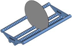 Single vertical substrate
 -
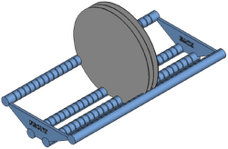 3 vertical substrates:
Dummy - Test - Dummy


For the 3 substrates only the center substrate was used for testing, the front and back wafers were used as dummy wafers. The wafers were placed in consecutive slots - when running multiple wafers in this way, the first and last wafers should always be dummy wafers.
The user manual, risk assessment, and contact information can be found in LabManager - requires login
Typical descum parameters
Tested with 1.5 µm AZ 5214E on 100 mm silicon substrate.
- O2: 100 sccm
- N2: 100 sccm
- Pressure (DSC): 1.3 mbar
- Power: 200 W
- Chamber temperature at start (with door closed): 30°C
- Time (single wafer): 5-10 minutes = 35-72 nm ashed
- Time (multiple wafers): 10-15 minutes = 40-80 nm ashed
| Single substrate | Center of 3 substrates | |
|---|---|---|
| Test results: ashing rate | 5.7 ±2.1 nm/min | 3.8 ±1.6 nm/min |
| Test results: non-uniformity | 0.6 ±0.4% | 0.4 ±0.2% |
| Wafers | 1 | 3 |
| Wafer size | 100 mm | 100 mm |
| Boat position | Center of chamber | Center of chamber |
| Test wafer position | Center of boat | Center of boat |
| Total gas flow rate | 200 sccm | 200 sccm |
| Gas mix ratio | 50% N2 | 50% N2 |
| Chamber pressure | 1.3 mbar | 1.3 mbar |
| Power | 200 W | 200 W |
| Test processing time | Tested parameter | Tested parameter |
| Test average temperature | 33°C | 33°C |
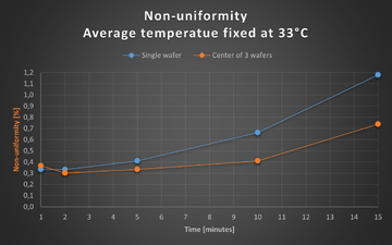
Single wafer descum ashing rate and uniformity for plasma asher 4 & 5

| Ashing time [min]: | 1 | 2 | 5 | 10 | 15 |
|---|---|---|---|---|---|
| Ashing amount [nm]: | 5.2 | 6.2 | 35.1 | 72.3 | 87.1 |
| Ashing rate [nm/min]: | 5.2 | 3.1 | 7.0 | 7.2 | 5.8 |
| Ashing time [min]: | 1 | 2 | 5 | 10 | 15 |
|---|---|---|---|---|---|
| Pre-descum film thickness range [nm]: | 11 | 12 | 10 | 11 | 9 |
| Pre-descum non-uniformity [%]: | 0.37 | 0.40 | 0.33 | 0.37 | 0.30 |
| Post-descum film thickness range [nm]: | 10 | 10 | 12 | 19 | 33 |
| Post-descum non-uniformity [%]: | 0.33 | 0.33 | 0.41 | 0.66 | 1.18 |
Multi wafer descum ashing rate and uniformity for plasma asher 4 & 5

| Ashing time [min]: | 1 | 2 | 5 | 10 | 15 |
|---|---|---|---|---|---|
| Ashing amount [nm]: | 4.3 | 6.7 | 10.1 | 39.5 | 78.8 |
| Ashing rate [nm/min]: | 4.3 | 3.4 | 2.0 | 4.0 | 5.3 |
| Ashing time [min]: | 1 | 2 | 5 | 10 | 15 |
|---|---|---|---|---|---|
| Pre-descum film thickness range [nm]: | 11 | 13 | 11 | 12 | 14 |
| Pre-descum non-uniformity [%]: | 0.37 | 0.43 | 0.37 | 0.40 | 0.46 |
| Post-descum film thickness range [nm]: | 11 | 9 | 10 | 12 | 21 |
| Post-descum non-uniformity [%]: | 0.37 | 0.30 | 0.33 | 0.41 | 0.74 |
Comparison between single substrate processing and multi substrate processing for plasma asher 4 & 5
Processing a single substrate using the standard descum settings will provide users with a relatively controllable and uniform process. Adding dummy substrates in close proximity with the process substrate will reduce the ashing rate and improve the uniformity:
-
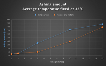 Ashing amount
 -
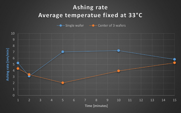 Ashing rate
 -
 Non-uniformity


Comparison of ashing rate between substrate sizes
It is assumed that the low power descum rates, for different substrate sizes, follows the same pattern as the high power ashing rates, which can be seen here.
Plasma Asher 5
Product name: PVA Tepla Gigabatch 380M
Year of purchase: 2024
Plasma asher 5 is identical to plasma asher 4, see descum processing for plasma asher 4 here.
Decommisioned tools
Plasma asher 1 was decommissioned 2024-12-02.
Information about decommissioned tool can be found here.
Plasma asher 2 was decommissioned 2024-12-02.