Specific Process Knowledge/Back-end processing/Laser Micromachining Tool: Difference between revisions
| (161 intermediate revisions by 6 users not shown) | |||
| Line 1: | Line 1: | ||
{{cc-nanolab}} | |||
'''Feedback to this page''': '''[mailto:labadviser@nanolab.dtu.dk?Subject=Feed%20back%20from%20page%20https://labadviser.nanolab.dtu.dk//index.php?title=Specific_Process_Knowledge/Back-end_processing/Laser_Micromachining_Tool click here]''' | |||
[[File: | ''All links to Kemibrug (SDS) and Labmanager Including APV and QC requires login.'' | ||
==Laser Micromachining Tool == | |||
[[File:LaserTool_photo.png|400px|thumb|Lasertool microSTRUCT vario (3D-Micromac AG)]] | |||
[[File:Inside_Camera_liveview.jpg|400px|thumb|Inside lasertool]] | [[File:Inside_Camera_liveview.jpg|400px|thumb|Inside lasertool]] | ||
| Line 11: | Line 14: | ||
The machine is located in the basement of building 346 under the cleanroom. | The machine is located in the basement of building 346 under the cleanroom. | ||
'''The user manual(s), user APV(s), technical information and contact information can be found in LabManager | '''The machine was upgraded with a high power femtosecond laser in January 2025.''' | ||
The information about the lasers below is therefor outdated. Those laser have been removed. | |||
The page will be updated very soon. | |||
'''The user manual(s), user APV(s), technical information and contact information can be found in [http://labmanager.danchip.dtu.dk/function.php?module=Machine&view=view&mach=309 LabManager]'''. | |||
<!-- remember to remove the type of documents that are not present --> | <!-- remember to remove the type of documents that are not present --> | ||
<!-- give the link to the equipment info page in LabManager: --> | <!-- give the link to the equipment info page in LabManager: --> | ||
It is equipped with 2 high power lasers: | It is equipped with 2 high power lasers: | ||
* a 50W picosecond laser that can emit light at 3 wavelengths: 355nm, 532nm and 1064nm (Time-Bandwidth Products, Fuego/Duetto. See some details in this | * a 50W picosecond laser that can emit light at 3 wavelengths: 355nm, 532nm and 1064nm (Time-Bandwidth Products, Fuego/Duetto. See some details in this [http://www.time-bandwidth.com/upload/press/weingartenlasertechnikjournalvol6issue3p51.pdf article]) with a pulse repetition rate from 200kHz up to 8000kHz. | ||
* a 100W nanosecond laser with a wavelength of 1064nm (IPG Laser YLP-HP series) with a pulse repetition rate of 100kHz (currently out of use). | |||
* a 100W nanosecond laser with a wavelength of 1064nm (IPG Laser YLP-HP series). | |||
The system is able to produce micro structures in different kinds of materials like metals, ceramics, composite materials, etc. | The system is able to produce micro structures in different kinds of materials like metals, ceramics, composite materials, etc. | ||
It can produce features down to ~10µm size over a large area. It can scan over an area of up to ~15x15cm without moving the sample. By moving the sample on the large x-y-stage this area can be extended by stitching. | It can produce features down to ~10µm size over a large area. It can scan over an area of up to ~15x15cm without moving the sample. By moving the sample on the large x-y-stage this area can be extended by stitching. | ||
== Process | The laser can use Autocad DXF files for the pattern design. To create these files we recommend to use Clewin 5. See more info [[Specific_Process_Knowledge/Pattern_Design| here]]. | ||
==Process Examples== | |||
A process example for cutting silicon grooves can be found [[/Silicon cutting and milling| <b>here</b>]]. | |||
== Technical specifications == | |||
*[[/Spot size and optics|Spot size and optics]] | |||
*[[/Lasers sources|Lasers sources]] | |||
== Performances == | |||
{| border="2" cellspacing="0" cellpadding="10" width="70%" | |||
|- | |||
!style="background:silver; color:black;" align="left"|Purpose | |||
|style="background:LightGrey; color:black"|Patterning, milling and dicing substrates | |||
|style="background:WhiteSmoke; color:black"|Mainly for patterning, milling, drilling with high aspect ratio and dicing substrate with micrometric shapes and above (> 10µm) | |||
|- | |||
!style="background:silver; color:black" align="left" valign="top" rowspan="4"|Performances | |||
|style="background:LightGrey; color:black"|Resolution | |||
|style="background:WhiteSmoke; color:black"| | |||
Down to 10µm with the blue laser (355nm). Depending on the depth wished. | |||
|- | |||
|style="background:LightGrey; color:black"|Maximum writing area | |||
|style="background:WhiteSmoke; color:black"| | |||
Depends of the optics. Max size : | |||
* Blue (145x145mm) | |||
* Green ( 165x165mm) | |||
* Red (165x165mm) | |||
|- | |||
|style="background:LightGrey; color:black"|Max. output power @100%(laser TB width – picosecond) | |||
|style="background:WhiteSmoke; color:black"| | |||
{| {{table}} | |||
| align="left"| | |||
{| border="1" cellspacing="1" cellpadding="2" align="left" style="width:600px" | |||
! Values from SAT (Nov. 2012) | |||
! Current values (Dec. 2018) | |||
|- | |||
| Repetition rate : 200kHz | |||
* 355nm, F103mm : 11,93W | |||
* 532nm, F255mm : 24,62W | |||
* 1064nm, F255mm : 34,24W | |||
Repetition rate : 1000 kHz | |||
* 355nm, F103mm : 4,28W | |||
* 532nm, F255mm : 18,40W | |||
* 1064nm, F255mm: 40,09W | |||
Repetition rate : 8000 kHz | |||
* 355nm, F103mm : 0,26W | |||
* 532nm, F255mm : 4,82W | |||
* 1064nm, F255mm : 42,40W | |||
| Repetition rate : 200 kHz | |||
* 355nm, F103mm : 15 W | |||
* 532nm, F255mm: not measured | |||
* 1064nm, F255mm: 32 W | |||
Repetition rate : 1000 kHz | |||
* 355nm, F103mm : 5,5 W | |||
* 532nm : not measured | |||
* 1064nm : 38 W | |||
Repetition rate : 8000 kHz | |||
* 355nm, F103mm: 0,3 W | |||
* 532nm, F255mm: not measured | |||
* 1064nm, F255mm: 41 W | |||
|} | |||
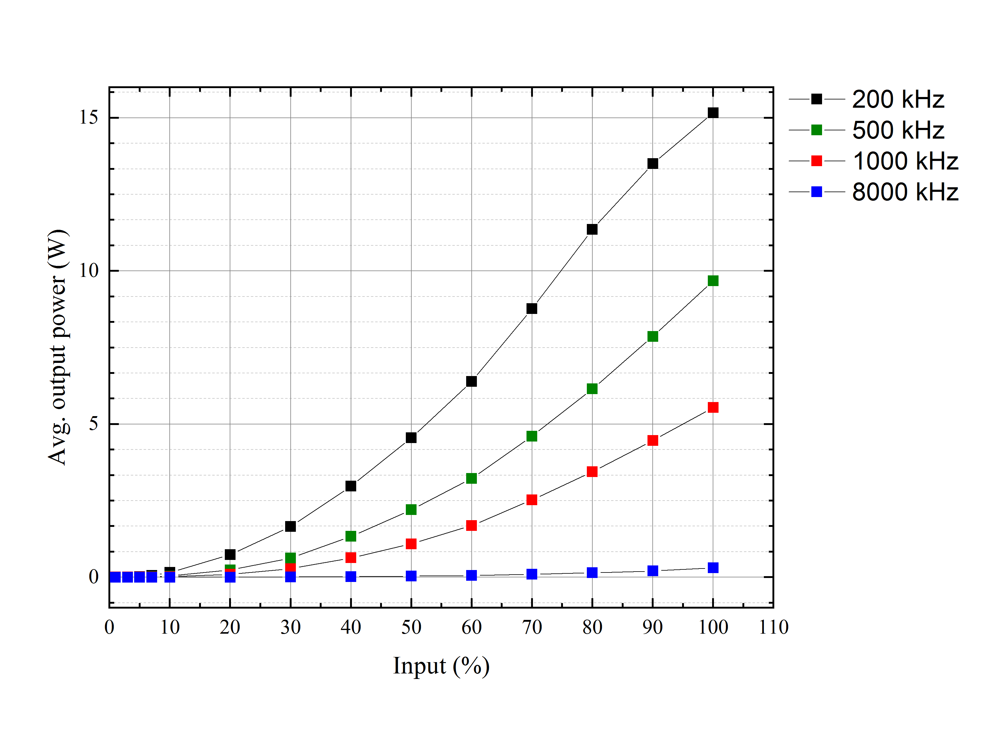
* [[Media:AvgPower 1064nm F255mm.png|Graph 1064nm, F255nm Avg. output power]] | |||
* [[Media:AvgPower 355nm F103mm.png|Graph 355nm, F103nm Avg. output power]] | |||
|} | |||
|- | |||
|style="background:LightGrey; color:black"|[[Media:140618 AverageOutputPower IPG.jpg|Output power@100%(laser IPG – nanosecond)]] | |||
|style="background:WhiteSmoke; color:black"| | |||
Repetition rate : 10kHz to 100kHz (Currently non-available) | |||
* 1064nm : 80W | |||
|- | |||
!style="background:silver; color:black" align="left" valign="top" rowspan="2"|Substrates | |||
|style="background:LightGrey; color:black"|Material allowed | |||
|style="background:WhiteSmoke; color:black"| | |||
* Silicon | |||
* Silicon + Si3N4 and/or SiO2 | |||
* Silicon with resist | |||
* Aluminum | |||
* Steel | |||
* Pyrex | |||
* Fused silicate (quartz) | |||
* Topas | |||
* Nickel | |||
* Tungsten | |||
* if not in the list ask machine responsible | |||
|- | |||
|style="background:LightGrey; color:black"|Material NOT allowed | |||
|style="background:WhiteSmoke; color:black"| | |||
* PTFE (teflon) | |||
|- | |||
!style="background:silver; color:black" align="left" valign="top" rowspan="1"|Parameters | |||
| style="background:LightGrey; color:black"|Characteristics | |||
|style="background:WhiteSmoke; color:black"| | |||
* Speed up to 2000 mm/s | |||
* M2 factor : <1.3 | |||
* Beam shape : Gaussian | |||
{| | |||
|- | |||
|} | |||
| align="center" | | |||
|} | |||
== Process information == | |||
=== Result from the acceptance test === | |||
=== Laser Processing | *[[/Laser Micromachining Tool acceptance test|Results from Laser Micromachining Tool acceptance test]] | ||
=== Laser Processing parameters === | |||
The following parameters provide information about the necessary values for machining different materials. However, most parameters can be further optimized in order to reduce the amount of debris and/or reduce the process time. | |||
<!-- | <!-- | ||
| Line 129: | Line 255: | ||
| 1 | | 1 | ||
| N/A | | N/A | ||
| [[ | | [[Media:Dicing Si 532nm f255mm.xls|Silicon dicing green parameters]] | ||
| Easily break silicon in cristal plan. Depth of the groove : 25µm | | Easily break silicon in cristal plan. Depth of the groove : 25µm | ||
|- style="background:LightGray;text-align:center" valign="top" | |- style="background:LightGray;text-align:center" valign="top" | ||
| Silicon (525µm) + Si3N4 (150nm to 1,2µm) OR SiO2 (150nm to 320nm) | | Silicon (525µm) + Si3N4 (150nm up to 1,2µm) OR SiO2 (150nm up to 320nm) | ||
| Red (1064nm/255mm) | | Red (1064nm/255mm) | ||
| 200 kHz | | 200 kHz | ||
| Line 143: | Line 269: | ||
| 4 | | 4 | ||
| 50 µm | | 50 µm | ||
| [[ | | [[Media:TB 1064nm 255mm cutting Si Si3N4.xls|Silicon nitride cutting parameters]] | ||
| Samples can easily be removed with a soft mechanical pressure. A layer of resist can be deposited on the top without influenced the dicing. | | Samples can easily be removed with a soft mechanical pressure. A layer of resist can be deposited on the top without influenced the dicing. Thicker layers (oxyde or nitride) have not been tested. | ||
|- | |- | ||
|- style="background:LightGray;text-align:center" valign="top" | |- style="background:LightGray;text-align:center" valign="top" | ||
| Line 158: | Line 284: | ||
| 1 | | 1 | ||
| N/A | | N/A | ||
| [[ | | [[Media:TB 532nm 255mm cutting Ni 320um.xls|Cutting Ni 320µm parameters]] | ||
| Cutting through only blue tape left | | Cutting through only blue tape left | ||
|- | |- | ||
|- style="background:LightGray;text-align:center" valign="top" | |- style="background:LightGray;text-align:center" valign="top" | ||
| Pyrex 1000µm | | Pyrex (1000µm) | ||
| Red(1064nm/255mm) | | Red(1064nm/255mm) | ||
| 200 kHz | | 200 kHz | ||
| Line 173: | Line 299: | ||
| 13 | | 13 | ||
| 20 µm | | 20 µm | ||
| [[ | | [[Media:TB 1064nm 255mm cutting pyrex microfluidic hole.xls|Cutting Pyrex 1000µm for microfluidic hole parameters]] | ||
| Increase/decrease the number of iteration to increase/decrease the width of the hole. [[ | | Increase/decrease the number of iteration to increase/decrease the width of the hole. [[Media:Pyrex 10um hole chanel.jpg|Microscope view of the chanel]] | ||
|- | |- | ||
|- style="background:LightGray;text-align:center" valign="top" | |- style="background:LightGray;text-align:center" valign="top" | ||
| Line 188: | Line 314: | ||
| 4 | | 4 | ||
| 20 µm | | 20 µm | ||
| [[ | | [[Media:TB 1064nm 255mm cutting Pyrex 525um.xls|Cutting Pyrex 525µm parameters]] | ||
| Cutting through. Dicing circle. | | Cutting through. Dicing circle. Can probably be optimized: 3 lines may be enough and half the iterations (tried by Azeem) | ||
|- | |||
|- style="background:LightGray;text-align:center" valign="top" | |||
| Steel (50µm) | |||
| Green(532nm/255mm) | |||
| 200 kHz | |||
| 20% | |||
| 0,55 W | |||
| 500 mm/s | |||
| 1 burst | |||
| 0 | |||
| 22 | |||
| | |||
| | |||
| [[Media:TB 532nm 255mm cutting shim steel 50um.xls|Cutting steel 50µm]] | |||
| Cutting shrim for Injection molder. | |||
|- | |||
|- style="background:LightGray;text-align:center" valign="top" | |||
| Steel (100µm) | |||
| Green(532nm/255mm) | |||
| 200 kHz | |||
| 25% | |||
| 0,55 W | |||
| 500 mm/s | |||
| 1 burst | |||
| 0 | |||
| 35 | |||
| | |||
| | |||
| [[Media:TB 532nm 255mm cutting shim steel 100um.xls|Cutting steel 100µm]] | |||
| Cutting shrim for Injection molder. | |||
|- | |||
|- style="background:LightGray;text-align:center" valign="top" | |||
| Steel (200µm) | |||
| Green(532nm/255mm) | |||
| 200 kHz | |||
| 25% | |||
| 0,55 W | |||
| 500 mm/s | |||
| 1 burst | |||
| 0 | |||
| 72 | |||
| | |||
| | |||
| [[Media:TB 532nm 255mm cutting shim steel 200um.xls|Cutting steel 200µm]] | |||
| Cutting shrim for Injection molder. | |||
|- | |||
|- style="background:LightGray;text-align:center" valign="top" | |||
| Aluminum (400µm) | |||
| Green(532nm/255mm) | |||
| 200 kHz | |||
| 100% | |||
| ?? W | |||
| 100 mm/s | |||
| 3 bursts | |||
| 0 | |||
| 35-40 | |||
| 4 | |||
| 20 | |||
| [[Media:Shaddowmask al lambda 532nm, F 255mm.xls|cutting Al 400µm]] | |||
| Cutting shadowmask for Wordentec. | |||
|- | |- | ||
|- style="background:LightGray;text-align:center" valign="top" | |||
| Aluminum (600µm) | |||
| Red IPG(1064nm/255mm) | |||
| 100 kHz | |||
| 100% | |||
| - W | |||
| 1000 mm/s | |||
| 1 bursts | |||
| 0 | |||
| 110 | |||
| 4 | |||
| 40 | |||
| [[Media:Aluminium cut IPG Lambda 1064nm, F 255mm.xls|cutting Al 600µm]] | |||
| Shadowmask. | |||
|} | |} | ||
The parameter filename extension is here set to .xls because of MediaWiki restrictions. The 3DMM laser software uses .par as parameter file extension. | |||
The parameter filename extension is here set to . | |||
The file should be a pure text-file with no formatting codes etc. | The file should be a pure text-file with no formatting codes etc. | ||
Latest revision as of 19:01, 27 May 2025
The content on this page, including all images and pictures, was created by DTU Nanolab staff, unless otherwise stated.
Feedback to this page: click here
All links to Kemibrug (SDS) and Labmanager Including APV and QC requires login.
Laser Micromachining Tool


The Laser Micromachining Tool is a microSTRUCT vario from the company 3D-Micromac AG.
The machine is located in the basement of building 346 under the cleanroom.
The machine was upgraded with a high power femtosecond laser in January 2025.
The information about the lasers below is therefor outdated. Those laser have been removed.
The page will be updated very soon.
The user manual(s), user APV(s), technical information and contact information can be found in LabManager.
It is equipped with 2 high power lasers:
- a 50W picosecond laser that can emit light at 3 wavelengths: 355nm, 532nm and 1064nm (Time-Bandwidth Products, Fuego/Duetto. See some details in this article) with a pulse repetition rate from 200kHz up to 8000kHz.
- a 100W nanosecond laser with a wavelength of 1064nm (IPG Laser YLP-HP series) with a pulse repetition rate of 100kHz (currently out of use).
The system is able to produce micro structures in different kinds of materials like metals, ceramics, composite materials, etc. It can produce features down to ~10µm size over a large area. It can scan over an area of up to ~15x15cm without moving the sample. By moving the sample on the large x-y-stage this area can be extended by stitching.
The laser can use Autocad DXF files for the pattern design. To create these files we recommend to use Clewin 5. See more info here.
Process Examples
A process example for cutting silicon grooves can be found here.
Technical specifications
Performances
| Purpose | Patterning, milling and dicing substrates | Mainly for patterning, milling, drilling with high aspect ratio and dicing substrate with micrometric shapes and above (> 10µm) | ||||
|---|---|---|---|---|---|---|
| Performances | Resolution |
Down to 10µm with the blue laser (355nm). Depending on the depth wished. | ||||
| Maximum writing area |
Depends of the optics. Max size :
| |||||
| Max. output power @100%(laser TB width – picosecond) |
| |||||
| Output power@100%(laser IPG – nanosecond) |
Repetition rate : 10kHz to 100kHz (Currently non-available)
| |||||
| Substrates | Material allowed |
| ||||
| Material NOT allowed |
| |||||
| Parameters | Characteristics |
|
Process information
Result from the acceptance test
Laser Processing parameters
The following parameters provide information about the necessary values for machining different materials. However, most parameters can be further optimized in order to reduce the amount of debris and/or reduce the process time.
| Material | Optics | Frequency | Intensity | Power measured @10% | Writing speed | Number of burst | Number of Z-offset | Number of iteration | Number of parallel lines | Gap in between line | Parameter file | Comments |
| Silicon 525µm | Green(532nm/255mm) | 200 kHz | 100% | 0,57 W | 50 mm/s | 1 burst | none | 4 | 1 | N/A | Silicon dicing green parameters | Easily break silicon in cristal plan. Depth of the groove : 25µm |
| Silicon (525µm) + Si3N4 (150nm up to 1,2µm) OR SiO2 (150nm up to 320nm) | Red (1064nm/255mm) | 200 kHz | 100% | 2,8 W | 1000 mm/s | 3 bursts | 1 (-0,3mm) | 350/100 | 4 | 50 µm | Silicon nitride cutting parameters | Samples can easily be removed with a soft mechanical pressure. A layer of resist can be deposited on the top without influenced the dicing. Thicker layers (oxyde or nitride) have not been tested. |
| Nickel (320µm) | Green(532nm/255mm) | 200 kHz | 100% | 0,64 W | 300 mm/s | 3 burst | none | 4320 | 1 | N/A | Cutting Ni 320µm parameters | Cutting through only blue tape left |
| Pyrex (1000µm) | Red(1064nm/255mm) | 200 kHz | 100% | 2,8 W | 1000 mm/s | 1 burst | none | 99 | 13 | 20 µm | Cutting Pyrex 1000µm for microfluidic hole parameters | Increase/decrease the number of iteration to increase/decrease the width of the hole. Microscope view of the chanel |
| Pyrex/Borosilicate glass (525µm) | Red(1064nm/255mm) | 200 kHz | 100% | 2,96 W | 1000 mm/s | 1 burst | 4 (-0,1/-0,2/-0,3/-0,4mm) | 300/500/700/900/1200 | 4 | 20 µm | Cutting Pyrex 525µm parameters | Cutting through. Dicing circle. Can probably be optimized: 3 lines may be enough and half the iterations (tried by Azeem) |
| Steel (50µm) | Green(532nm/255mm) | 200 kHz | 20% | 0,55 W | 500 mm/s | 1 burst | 0 | 22 | Cutting steel 50µm | Cutting shrim for Injection molder. | ||
| Steel (100µm) | Green(532nm/255mm) | 200 kHz | 25% | 0,55 W | 500 mm/s | 1 burst | 0 | 35 | Cutting steel 100µm | Cutting shrim for Injection molder. | ||
| Steel (200µm) | Green(532nm/255mm) | 200 kHz | 25% | 0,55 W | 500 mm/s | 1 burst | 0 | 72 | Cutting steel 200µm | Cutting shrim for Injection molder. | ||
| Aluminum (400µm) | Green(532nm/255mm) | 200 kHz | 100% | ?? W | 100 mm/s | 3 bursts | 0 | 35-40 | 4 | 20 | cutting Al 400µm | Cutting shadowmask for Wordentec. |
| Aluminum (600µm) | Red IPG(1064nm/255mm) | 100 kHz | 100% | - W | 1000 mm/s | 1 bursts | 0 | 110 | 4 | 40 | cutting Al 600µm | Shadowmask. |
The parameter filename extension is here set to .xls because of MediaWiki restrictions. The 3DMM laser software uses .par as parameter file extension.
The file should be a pure text-file with no formatting codes etc.