Specific Process Knowledge/Lithography/Pretreatment: Difference between revisions
| (36 intermediate revisions by 2 users not shown) | |||
| Line 1: | Line 1: | ||
{{cc-nanolab}} | |||
[[Category: Equipment | | '''Feedback to this page''': '''[mailto:labadviser@nanolab.dtu.dk?Subject=Feed%20back%20from%20page%20http://labadviser.nanolab.dtu.dk/index.php/Specific_Process_Knowledge/Lithography/Pretreatment click here]''' | ||
[[Category: Equipment|Pretreatment]] | |||
[[Category: Lithography|Pretreatment]] | [[Category: Lithography|Pretreatment]] | ||
| Line 16: | Line 18: | ||
==HMDS== | ==HMDS== | ||
In the HMDS priming process, the -OH groups on the surface of the substrate are replaced with Si(CH<sub>3</sub>)<sub>3</sub>, thus changing the surface from hydrophilic to (more) hydrophobic. Substrates with surfaces of silicon or | In the HMDS priming process, the -OH groups on the surface of the substrate are replaced with Si(CH<sub>3</sub>)<sub>3</sub>, thus changing the surface from hydrophilic to (more) hydrophobic. Substrates with surfaces of silicon, or its oxides/nitrides, all work very well with HMDS pretreatment. | ||
Other semiconductors, insulators, or metals that form -OH groups on the surface may be suitable as well. The shelf life of substrates primed using HMDS (vapor phase) is long, maybe even several weeks. | |||
==Dip/spin-on adhesion promoter== | ==Dip/spin-on adhesion promoter== | ||
| Line 26: | Line 30: | ||
==Comparing pretreatment methods== | ==Comparing pretreatment methods== | ||
{|border="1" cellspacing="1" cellpadding=" | {|border="1" cellspacing="1" cellpadding="10" style="text-align:left;" | ||
|- | |- | ||
| Line 32: | Line 36: | ||
|-style="background:silver; color:black" | |-style="background:silver; color:black" | ||
! | ! | ||
![[Specific Process Knowledge/Lithography/Pretreatment# | ![[Specific Process Knowledge/Lithography/Pretreatment#HMDS_2|HMDS]] | ||
![[Specific Process Knowledge/Lithography/Pretreatment#Buffered HF-Clean|Buffered HF-Clean]] | ![[Specific Process Knowledge/Lithography/Pretreatment#Buffered HF-Clean|Buffered HF-Clean]] | ||
![[Specific Process Knowledge/Lithography/Pretreatment#Oven 250C|Oven 250C]] | ![[Specific Process Knowledge/Lithography/Pretreatment#Oven 250C|Oven 250C]] | ||
| Line 96: | Line 100: | ||
|-style="background:WhiteSmoke; color:black" | |-style="background:WhiteSmoke; color:black" | ||
!Restrictions | !Restrictions | ||
| | |Low Tg polymer substrates, type IV films, and resist/polymer on substrate | ||
i.e. no resist coated wafers or | i.e. no resist coated wafers or Crystalbonded chips! | ||
|Wafers with metal is not allowed | |Wafers with metal is not allowed | ||
|Resist is not allowed | |Resist is not allowed | ||
| Line 113: | Line 117: | ||
Overview of what pretreatment is used for various surfaces at DTU Nanolab. Parentheses () indicate the method is not the optimal choice, or that the information is taken from product information supplied by manufacturers. | Overview of what pretreatment is used for various surfaces at DTU Nanolab. Parentheses () indicate the method is not the optimal choice, or that the information is taken from product information supplied by manufacturers. | ||
{|border="1" cellspacing="1" cellpadding=" | |||
{|border="1" cellspacing="1" cellpadding="10" style="text-align:left;" | |||
|- | |- | ||
| Line 242: | Line 247: | ||
=HMDS= | =HMDS= | ||
The chemical treatment with hexamethyldisilazane (HMDS) before the spin coating can be used to promote the adhesion for photoresist. Vapor priming with HMDS leaves a mono-layer of TMS (trimethylsilyl) on the Si or SiO<sub>2</sub> surface. The process dehydrates the substrate surface, and lowers the surface | The chemical treatment with hexamethyldisilazane (HMDS) before the spin coating can be used to promote the adhesion for photoresist. Vapor priming with HMDS leaves a mono-layer of TMS (trimethylsilyl) on the Si or SiO<sub>2</sub> surface. The process dehydrates the substrate surface, and lowers the surface energy to promote better wetting. | ||
The molecular formula for hexamethyldisilazane, or bis(trimethylsilyl)amine, is C<sub>6</sub>H<sub>19</sub>NSi<sub>2</sub> | The molecular formula for hexamethyldisilazane, or bis(trimethylsilyl)amine, is C<sub>6</sub>H<sub>19</sub>NSi<sub>2</sub>. | ||
[[ | [[File:HMDS priming schematic.png|400px|thumb|right|Schematic of the HMDS vapor priming process]] | ||
<br clear="all" /> | <br clear="all" /> | ||
| Line 252: | Line 257: | ||
==Comparing HMDS priming== | ==Comparing HMDS priming== | ||
{| border=" | {|border="1" cellspacing="1" cellpadding="10" style="text-align:left;" | ||
!colspan="2" border="none" style="background:silver; color:black;" align="center"|Equipment | !colspan="2" border="none" style="background:silver; color:black;" align="center"|Equipment | ||
| Line 305: | Line 310: | ||
|style="background:WhiteSmoke; color:black"| | |style="background:WhiteSmoke; color:black"| | ||
1 min / wafer | 1-2 min / wafer | ||
|- | |- | ||
| Line 361: | Line 366: | ||
==Oven: HMDS 2== | ==Oven: HMDS 2== | ||
[[Image:HMDS2.jpg| | [[Image:HMDS2.jpg|400px|thumb|The Oven: HMDS 2 oven is located in E-5.]] | ||
The user manual, user APV, and contact information can be found in LabManager: | |||
[http://labmanager.dtu.dk/function.php?module=Machine&view=view&mach=358 Oven: HMDS 2] - '''requires login''' | |||
'''Process information:''' | '''Process information:''' | ||
*Recipe 1: baseline prime process with 5 min HMDS priming time | *Recipe 1: baseline prime process with 5 min HMDS priming time | ||
| Line 374: | Line 379: | ||
==Spin Coater: Gamma UV== | ==Spin Coater: Gamma UV== | ||
[[Image:HMDS gammaUV.jpg| | [[Image:HMDS gammaUV.jpg|400px|thumb|HMDS module (top) in Spin Coater: Gamma UV in E-5.]] | ||
The user manual, user APV, and contact information can be found in LabManager: | |||
[http://labmanager.dtu.dk/function.php?module=Machine&view=view&mach=359 Spincoater: Gamma UV] | [http://labmanager.dtu.dk/function.php?module=Machine&view=view&mach=359 Spincoater: Gamma UV] - '''requires login''' | ||
Additional information about the spin coater and processes can be found in Labadviser: | |||
[http://labadviser.nanolab.dtu.dk/index.php/Specific_Process_Knowledge/Lithography/Coaters#Spin_Coater:_Gamma_UV Spin Coater: Gamma UV] | [http://labadviser.nanolab.dtu.dk/index.php/Specific_Process_Knowledge/Lithography/Coaters#Spin_Coater:_Gamma_UV Spin Coater: Gamma UV] | ||
| Line 389: | Line 394: | ||
==Spin Coater: Gamma e-beam & UV== | ==Spin Coater: Gamma e-beam & UV== | ||
[[image:Gamma_4M_-_E-beam_&_UV_full.JPG| | [[image:Gamma_4M_-_E-beam_&_UV_full.JPG|400px|thumb|Spin Coater: Gamma e-beam & UV in E-5.]] | ||
The user manual, user APV, and contact information can be found in LabManager: | |||
[http://labmanager.dtu.dk/function.php?module=Machine&view=view&mach= | [http://labmanager.dtu.dk/function.php?module=Machine&view=view&mach=417 Spin Coater: Gamma e-beam & UV] - '''requires login''' | ||
Additional information about the spin coater and processes can be found in Labadviser: | |||
[http://labadviser.nanolab.dtu.dk/index.php/Specific_Process_Knowledge/Lithography/Coaters#Spin_Coater:_Gamma_E-beam_and_UV Spin Coater: Gamma e-beam & UV] | [http://labadviser.nanolab.dtu.dk/index.php/Specific_Process_Knowledge/Lithography/Coaters#Spin_Coater:_Gamma_E-beam_and_UV Spin Coater: Gamma e-beam & UV] | ||
| Line 403: | Line 408: | ||
=Buffered HF-Clean= | =Buffered HF-Clean= | ||
[[image:BHF clean.JPG| | [[image:BHF clean.JPG|400px|thumb||BHF clean wetbench 04 in D-3.]] | ||
Another commonly used method to render the surface of silicon wafers hydrophobic is the dilute HF dip. | Another commonly used method to render the surface of silicon wafers hydrophobic is the dilute HF dip. | ||
| Line 410: | Line 415: | ||
The native oxide layer will be removed by 30 seconds of etching and this will promote the resist adhesion on the Si substrates. We recommend to spin coat resist as soon as possible after the procedure. | The native oxide layer will be removed by 30 seconds of etching and this will promote the resist adhesion on the Si substrates. We recommend to spin coat resist as soon as possible after the procedure. | ||
[https://labmanager.dtu.dk/function.php?module=Machine&view=view&mach=378 Buffered HF-Clean in LabManager] | The user manual, user APV, and contact information can be found in LabManager: | ||
[https://labmanager.dtu.dk/function.php?module=Machine&view=view&mach=378 Buffered HF-Clean in LabManager] - '''requires login''' | |||
Additional information about the spin coater and processes can be found in Labadviser: | |||
[[Specific Process Knowledge/Etch/Wet Silicon Oxide Etch (BHF)|Wet Silicon Oxide Etch (BHF)]] | [[Specific Process Knowledge/Etch/Wet Silicon Oxide Etch (BHF)|Wet Silicon Oxide Etch (BHF)]] | ||
<br clear="all" /> | <br clear="all" /> | ||
{{:Specific Process Knowledge/Lithography/Pretreatment/Oven_250C}} | |||
Latest revision as of 15:01, 22 April 2025
The content on this page, including all images and pictures, was created by DTU Nanolab staff, unless otherwise stated.
Feedback to this page: click here
Pretreatment
Pretreatment, also known as priming, is done before spin coating in order to ensure the best conditions for adhesion between the substrate surface and the resist. Pretreatment ranges from a simple dehydration bake over etching the native oxide to vapor phase deposition of an adhesion promoter. The goal of pretreatment is to remove any moisture that may be adsorbed on the surface of the substrate, and/or to modify the contact angle of the surface to match that of the resist to be coated on the substrate.
All surfaces can be divided to hydrophilic or hydrophobic surfaces. Oxidized surfaces such as SiO2 or surfaces with native oxide (e.g. Si or Al substrates) are considered to be hydrophilic and have very bad wetting with hydrophobic resist. The adhesion of most resists on hydrophilic surfaces is deteriorated if moisture is present on the surface. Therefore it is very important to do the pretreatment step before spin coating. This page gives an overview of treatments available at DTU Nanolab to promote photoresist adhesion.
Dehydration
A dehydration bake immediately before spin coating removes the moisture adsorbed to the surface, and greatly improves the adhesion of resist on most surfaces. For thin hydrophilic layers, a few minutes on a hotplate at or above 100°C may suffice. For thicker layers or bulk oxide samples, a dehydration bake at 250°C over night is recommended. Due to the moisture in the cleanroom atmosphere, this priming naturally has a short shelf life, so spin coating should be done as soon as possible.
BHF dip
Stripping the native oxide using BHF only works if the native oxide of the substrate is etched by BHF, and if resist has good adhesion to the substrate material itself, which basically limits it to silicon. A BHF dip leaves the surface of a silicon wafer hydrophobic, and the dangling Si-bonds are passivated by adsorbed H+. This means the surface will not oxidize immediately, but the lifetime of this passivation is limited, so it is recommended to spin coat the wafer within 20, maximum 45 minutes.
HMDS
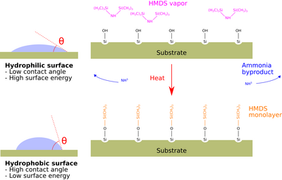
In the HMDS priming process, the -OH groups on the surface of the substrate are replaced with Si(CH3)3, thus changing the surface from hydrophilic to (more) hydrophobic. Substrates with surfaces of silicon, or its oxides/nitrides, all work very well with HMDS pretreatment.
Other semiconductors, insulators, or metals that form -OH groups on the surface may be suitable as well. The shelf life of substrates primed using HMDS (vapor phase) is long, maybe even several weeks.
Dip/spin-on adhesion promoter
Adhesion promoters for dip or spin-on application are commercially available. Most are solvent based with some, usually proprietary, additives. They work by first cleaning the substrate surface, and subsequently priming the surface with the additives as the solvent evaporates.
Hard bake
If the adhesion between the substrate surface and the resist is sufficient to survive the development process without delamination, the adhesion in subsequent process steps can be improved by a so-called hard bake. Baking the substrate a few minutes on a hotplate (or approx. half an hour in a convection oven) at a temperature higher than the soft bake temperature, e.g. 110-130°C, usually improves the adhesion between resist and surface. Depending on the type of resist used, and the temperature of the hard bake, reflow of the resist pattern may be a side effect.
Comparing pretreatment methods
| HMDS | Buffered HF-Clean | Oven 250C | |
|---|---|---|---|
| Generel description |
Vapor priming |
Native oxide strip |
Dehydration |
| Chemical |
hexamethyldisilazane (HMDS) |
12%HF with Ammoniumflouride |
none |
| Substrate size |
|
|
|
| Allowed materials |
Silicon, glass, and polymer substrates (Tg > 150°C) Film or pattern of all types, except type IV and resist/polymer |
|
|
| Restrictions | Low Tg polymer substrates, type IV films, and resist/polymer on substrate
i.e. no resist coated wafers or Crystalbonded chips! |
Wafers with metal is not allowed | Resist is not allowed |
Pretreatment of various surfaces
General comment regarding III-V materials:
A dehydration bake prior to spin coating can be enough, especially if adhesion is not critical, and if the resist is not left more than a day or two on the surface. Application of dip/spin-on adhesion promoter can improve the adhesion and shelf life. If adhesion is critical in the subsequent process step, application of a thin layer of SiO2 using PECVD (followed by HMDS priming) as an adhesion layer is recommended.
Overview of what pretreatment is used for various surfaces at DTU Nanolab. Parentheses () indicate the method is not the optimal choice, or that the information is taken from product information supplied by manufacturers.
| Dehydration | BHF dip | HMDS | Dip/spin-on adhesion promoter | Comment | |
| Silicon with native oxide | (X) | X | X | (X) | |
| Silicon oxide | (X) | X | (X) | ||
| Silicon nitride | (X) | X | (X) | ||
| Glass (borofloat/pyrex) | X | X | (X) | Dehydration before HMDS is probably best | |
| Fused silica (quartz) | X | X | (X) | Dehydration before HMDS is probably best | |
| InGaAs | (X) | SurPass 3000 | |||
| GaAs | (X) | SurPass 3000 | |||
| GaP | (X) | ? | AR800-30 is being tested (leaves residue) | ||
| InP | (X) | ? | AR800-30 is being tested (leaves residue) | ||
| GaN | (X) | ? | |||
| InN | (X) | ? |
The information on III-V materials has been provided by Kresten Yvind at DTU Fotonik June 2021.
HMDS
The chemical treatment with hexamethyldisilazane (HMDS) before the spin coating can be used to promote the adhesion for photoresist. Vapor priming with HMDS leaves a mono-layer of TMS (trimethylsilyl) on the Si or SiO2 surface. The process dehydrates the substrate surface, and lowers the surface energy to promote better wetting.
The molecular formula for hexamethyldisilazane, or bis(trimethylsilyl)amine, is C6H19NSi2.

Comparing HMDS priming
| Equipment | Oven: HMDS 2 | Gamma UV/ Gamma e-beam and UV | |||
|---|---|---|---|---|---|
| Purpose |
|
| |||
| Priming chemical |
hexamethyldisilazane (HMDS) | ||||
| Performance | Contact angle |
|
Fast recipe [standard recipe]:
| ||
| Process parameters | Process temperature |
150°C |
120°C | ||
| Process time |
25 minutes |
1-2 min / wafer | |||
| Substrates | Substrate size |
|
| ||
| Allowed materials |
Silicon, glass, and polymer substrates III-V materials on silicon carrier Film or pattern of all but types, except type IV and resist/polymer (incl. Crystalbond) |
Silicon and glass wafers Film or pattern of all but types, except type IV and resist/polymer (incl. Crystalbond) | |||
| Batch |
1 - 25, multiple batches possible |
1 - 25 | |||
Contact angle:
The contact angle of the substrate surface can be measured using the Drop Shape Analyzer.
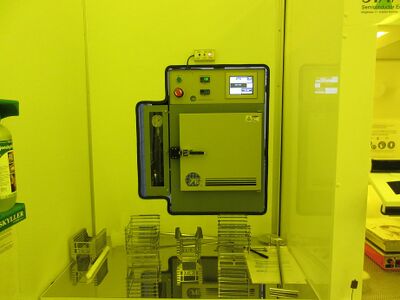
Oven: HMDS 2

The user manual, user APV, and contact information can be found in LabManager:
Oven: HMDS 2 - requires login
Process information:
- Recipe 1: baseline prime process with 5 min HMDS priming time
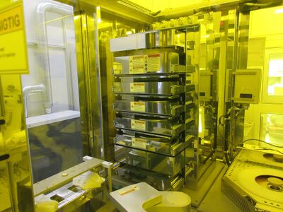
Spin Coater: Gamma UV

The user manual, user APV, and contact information can be found in LabManager:
Spincoater: Gamma UV - requires login
Additional information about the spin coater and processes can be found in Labadviser:
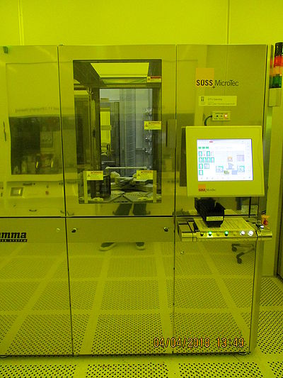
Spin Coater: Gamma e-beam & UV

The user manual, user APV, and contact information can be found in LabManager:
Spin Coater: Gamma e-beam & UV - requires login
Additional information about the spin coater and processes can be found in Labadviser:
Spin Coater: Gamma e-beam & UV
Buffered HF-Clean

Another commonly used method to render the surface of silicon wafers hydrophobic is the dilute HF dip.
BHF is mostly used to do pretreatment for new Si wafers.
The native oxide layer will be removed by 30 seconds of etching and this will promote the resist adhesion on the Si substrates. We recommend to spin coat resist as soon as possible after the procedure.
The user manual, user APV, and contact information can be found in LabManager:
Buffered HF-Clean in LabManager - requires login
Additional information about the spin coater and processes can be found in Labadviser:
Oven 250C

The oven is typically used for dehydration pretreatment, of Si and glass substrates, to promote the resist adhesion. We recommend placing the wafers in a metal carrier in the oven for at least for 4 hours, or overnight, and spin coat resist on them as soon as possible after removing them from the oven.
The user manual, and contact information can be found in LabManager:
Oven 250C - requires login
