Specific Process Knowledge/Lithography/nLOF: Difference between revisions
| (13 intermediate revisions by 2 users not shown) | |||
| Line 1: | Line 1: | ||
{{:Specific Process Knowledge/Lithography/authors_generic}} | |||
'''Feedback to this page''': '''[mailto:labadviser@nanolab.dtu.dk?Subject=Feed%20back%20from%20page%20http://labadviser.nanolab.dtu.dk/index.php/Specific_Process_Knowledge/Lithography/nLOF click here]''' | |||
[[Category: Lithography|Resist]] | |||
[[Category: Resist|AZ nLOF 2020]] | |||
__TOC__ | __TOC__ | ||
| Line 18: | Line 25: | ||
*PEB time: 60 s | *PEB time: 60 s | ||
The recommended PEB for nLOF is 60 seconds at 110°C, regardless of resist film thickness. | |||
===PEB baking time investigation=== | |||
While 60 s @ 110°C is adequate for Si substrates, less thermally conductive substrates (glass, III-V materials, chips bonded to carrier), have shown problems using the standard PEB recipe.<br> | |||
These problems were largely solved by increasing the PEB time to 120 s. Tests (on Aligner: Maskless 02) have shown that the lithographic performance of nLOF on Si is improved when using 120 s @ 110°C PEB (less stitching, less bias, more negative profile). | |||
A small report on the tests can be found here: [[media:nLOF_PEBtime_2019.pdf|'''nLOF PEB time 2019''']]. | |||
==Development== | ==Development== | ||
| Line 30: | Line 37: | ||
*Puddle development in 2.38% TMAH (AZ 726 MIF): ~4 µm/min | *Puddle development in 2.38% TMAH (AZ 726 MIF): ~4 µm/min | ||
A 2 µm nLOF resist film is fully developed in ~30 s in 2.38% TMAH (AZ 726 MIF). However, the development can be continued to 60 s in order to get a more negative resist profile (due to increased under-cut). | |||
===Solvent development=== | |||
Cross-linking negative resists have the potential to be developed using organic solvents instead of the normally used alkaline aqueous solutions. A quick test of this was carried out by Thomas Anhøj @ DTU Nanolab, showing that nLOF 2020 could potentially be used for water-free lithography. | |||
A | A small report on the test can be found here: [[media:nLOF_solventdev_2024.pdf|'''nLOF solvent development 2024''']]. | ||
Latest revision as of 09:13, 9 April 2025
Feedback to this page: click here
Resist description
AZ nLOF 2020 is a negative UV photoresist, suitable for lift-off processes.
Spin coating

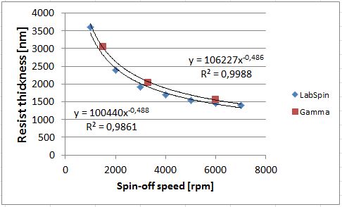
Typical spin parameters:
- Spin off: 30-60 s
- Soft bake: 60 s @ 110°C
Post-exposure bake
Typical PEB parameters:
- PEB temperature: 110°C
- PEB time: 60 s
The recommended PEB for nLOF is 60 seconds at 110°C, regardless of resist film thickness.
PEB baking time investigation
While 60 s @ 110°C is adequate for Si substrates, less thermally conductive substrates (glass, III-V materials, chips bonded to carrier), have shown problems using the standard PEB recipe.
These problems were largely solved by increasing the PEB time to 120 s. Tests (on Aligner: Maskless 02) have shown that the lithographic performance of nLOF on Si is improved when using 120 s @ 110°C PEB (less stitching, less bias, more negative profile).
A small report on the tests can be found here: nLOF PEB time 2019.
Development
Development speed:
- Puddle development in 2.38% TMAH (AZ 726 MIF): ~4 µm/min
A 2 µm nLOF resist film is fully developed in ~30 s in 2.38% TMAH (AZ 726 MIF). However, the development can be continued to 60 s in order to get a more negative resist profile (due to increased under-cut).
Solvent development
Cross-linking negative resists have the potential to be developed using organic solvents instead of the normally used alkaline aqueous solutions. A quick test of this was carried out by Thomas Anhøj @ DTU Nanolab, showing that nLOF 2020 could potentially be used for water-free lithography.
A small report on the test can be found here: nLOF solvent development 2024.
