Specific Process Knowledge/Lithography: Difference between revisions

From LabAdviser
Jehem (talk | contribs)
Tag: Manual revert
Jehem (talk | contribs)
 
(10 intermediate revisions by the same user not shown)
Line 105: Line 105:
=Equipment and Process Pages=


{| style="color: black;" width="90%"
{{:Specific Process Knowledge/Lithography/UVlithographyProcessPages}}
| colspan="3" |
|-
| style="width: 20%"|
'''<big>[[Specific Process Knowledge/Lithography/Resist|Resist]]</big>'''
*[[Specific_Process_Knowledge/Lithography/Resist#User_resist_bottles_in_the_cleanroom|User bottles in the cleanroom]]
*[[Specific_Process_Knowledge/Lithography/Resist#UV_Resist|UV Resist]]
*[[Specific_Process_Knowledge/Lithography/Resist#DUV_Resist|DUV Resist]]
*[[Specific_Process_Knowledge/Lithography/Resist#E-beam_Resist|E-beam Resist]]
*[[Specific_Process_Knowledge/Lithography/Resist#Imprint_Resist|Imprint Resist]]
 
'''<big>[[Specific Process Knowledge/Lithography/Pretreatment|Pretreatment]]</big>'''
*[[Specific Process Knowledge/Lithography/Pretreatment#HMDS|HMDS]]
*[[Specific Process Knowledge/Lithography/Pretreatment#Buffered_HF-Clean|BHF]]
*[[Specific_Process_Knowledge/Lithography/Pretreatment#Oven_250C|Oven 250C]]
 
'''<big>[[Specific Process Knowledge/Lithography/Coaters|Coating]]</big>'''
*[[Specific_Process_Knowledge/Lithography/Coaters#Spin_Coater:_Gamma_UV|Spin Coater: Gamma UV]]
*[[Specific Process Knowledge/Lithography/DUVStepperLithography#SÜSS Spinner-Stepper|Spin Coater: Süss Stepper]]
*[[Specific_Process_Knowledge/Lithography/Coaters#Spin_Coater:_Gamma_E-beam_and_UV|Spin Coater: Gamma e-beam & UV]]
*[[Specific Process Knowledge/Lithography/Coaters#Spin_Coater:_RCD8|Spin Coater: RCD8]]
*[[Specific_Process_Knowledge/Lithography/Coaters#Spin_coater:_Labspin|Spin Coater: Labspin 02/03]]
*[[Specific_Process_Knowledge/Lithography/Coaters/SprayCoater|Spray Coater]]
 
'''<big>[[Specific Process Knowledge/Lithography/Baking|Baking]]</big>'''
*[[Specific Process Knowledge/Lithography/Baking#Hotplates|Hotplates]]
*[[Specific Process Knowledge/Lithography/Baking#Ovens|Ovens]]
 
| style="width: 20%"; valign="top"|
'''<big>[[Specific Process Knowledge/Lithography/UVExposure|UV Exposure Tools]]</big>'''
*[[Specific_Process_Knowledge/Lithography/UVExposure#Aligner:_MA6-1|Aligner: MA6-1]]
*[[Specific_Process_Knowledge/Lithography/UVExposure#Aligner:_MA6-2|Aligner: MA6-2]]
<!--*[[Specific Process Knowledge/Lithography/UVExposure#Inclined UV lamp|Inclined UV-lamp]]-->
*[[Specific Process Knowledge/Lithography/UVExposure#Aligner: Maskless 01|Aligner: Maskless 01]]
*[[Specific Process Knowledge/Lithography/UVExposure#Aligner: Maskless 02|Aligner: Maskless 02]]
*[[Specific_Process_Knowledge/Lithography/UVExposure#Aligner:_Maskless_03|Aligner: Maskless 03]]
*[[Specific_Process_Knowledge/Lithography/UVExposure#Aligner:_Maskless_04|Aligner: Maskless 04]]
 
'''<big>[[Specific_Process_Knowledge/Lithography/DUVStepperLithography|Deep-UV Exposure]]</big>'''
*[[Specific_Process_Knowledge/Lithography/DUVStepperLithography#DUV_Stepper|DUV Stepper (Canon FPA-3000EX4)]]
 
'''<big>[[Specific Process Knowledge/Lithography/EBeamLithography|Electron Beam Exposure]]</big>'''
*[[Specific_Process_Knowledge/Lithography/EBeamLithography/JEOL_9500_User_Guide|JEOL 9500]]
*[[Specific_Process_Knowledge/Lithography/EBeamLithography/eLINE|Raith Eline]]
 
'''<big>[[Specific_Process_Knowledge/Imprinting|Nano Imprint Lithography]]</big>'''
*[[Specific Process Knowledge/Thin film deposition/MVD|Molecular Vapour Deposition]]
*[[Specific Process Knowledge/Lithography/NanoImprintLithography#EVG NIL|Imprinter 01]]
 
 
| style="width: 20%"; valign="top"|
'''<big>[[Specific Process Knowledge/Lithography/Development|Development]]</big>'''
*[[Specific_Process_Knowledge/Lithography/Development#Manual_beaker_development_in_fumehood|Manual beaker development]]
*[[Specific_Process_Knowledge/Lithography/Development#Developer:_SU8_(Wet_Bench)|Developer: SU8 (Wetbench)]]
*[[Specific_Process_Knowledge/Lithography/Development#Developer:_E-beam_02|Developer: E-beam 02]]
*[[Specific_Process_Knowledge/Lithography/Development#Developer:_TMAH_Manual_02|Developer: TMAH Manual 02]]
*[[Specific_Process_Knowledge/Lithography/Development#Developer_TMAH_UV-lithography|Developer: TMAH UV-lithography]]
*[[Specific_Process_Knowledge/Lithography/DUVStepperLithography#Developer:_TMAH_Stepper|Developer: TMAH Stepper]]
 
'''<big>[[Specific Process Knowledge/Lithography/Descum|Descum]]</big>'''
*[[Specific Process Knowledge/Lithography/Descum#Plasma_Asher_3:_Descum|Plasma Asher 3: Descum]]
*[[Specific Process Knowledge/Lithography/Descum#Plasma_Asher_4|Plasma Asher 4]]
*[[Specific Process Knowledge/Lithography/Descum#Plasma_Asher_5|Plasma Asher 5]]
*[[Specific_Process_Knowledge/Etch/Wet_Silicon_Oxide_Etch_(BHF)|BHF]]
 
'''<big>[[Specific Process Knowledge/Lithography/LiftOff|Lift-off]]</big>'''
*[[Specific Process Knowledge/Lithography/LiftOff#Lift-off_wet_bench_07|Lift-off]]
 
'''<big>[[Specific Process Knowledge/Lithography/Strip|Strip]]</big>'''
*[[Specific Process Knowledge/Lithography/Strip#Plasma_Asher_3: Descum|Plasma Asher 3: Descum]]
*[[Specific Process Knowledge/Lithography/Strip#Plasma_Asher_4|Plasma Asher 4]]
*[[Specific Process Knowledge/Lithography/Strip#Plasma_Asher_5|Plasma Asher 5]]
*[[Specific Process Knowledge/Lithography/Strip#Resist_Strip|Resist Strip]]
|}
<br clear="all" />


=Lithography Tool Package Training=

Latest revision as of 17:06, 2 April 2025

The contents on this page, including all images and pictures, was created by DTU Nanolab staff unless otherwise stated.

Feedback to this page: click here

Lithography
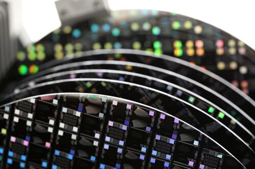
Lithography is a method used for transferring a pattern from a physical or digital mask onto the substrate. At DTU Nanolab we have four different types of lithography available:


Comparing lithography methods at DTU Nanolab

UV Lithography DUV Stepper Lithography E-beam Lithography Nano Imprint Lithography
Generel description Pattern transfer via ultraviolet (UV) light Pattern transfer via deep ultraviolet (DUV) light Patterning by electron beam Pattern transfer via hot embossing (HE)
Pattern size range ~1 µm and up
(resist type, thickness, and pattern dependent)
~200 nm and up
(pattern type, shape and pitch dependent)
~10-1000 nm
(and larger at high currents)
~20 nm and up
Resist type

UV sensitive:

  • AZ 5214E, AZ 4562, AZ MiR 701 (positive)
  • AZ 5214E, AZ nLOF 2020, SU-8 (negative)

DUV sensitive:

  • JSR KRF M230Y, JSR KRF M35G (positive)
  • UVN2300-0.8 (negative)

E-beam sensitive:

  • AR-P6200 CSAR, ZEP502A , PMMA (positive)
  • HSQ, mr-EBL, AR-N 7520 (negative)

Imprint polymers:

  • Topas
  • PMMA
  • mr-I 7030R
Resist thickness range ~0.5 µm to 200 µm ~50 nm to 2 µm ~30 nm to 1 µm ~100 nm to 2 µm
Typical exposure time Mask aligner: 10-180 s per wafer
Maskless aligner: 5-60 minutes per wafer

Process dependent:

  • Pattern
  • Pattern area
  • Dose

Throughput is up to 60 wafers/hour

Process dependent:

  • Dose [µC/cm2]:
  • Beam current [A]:
  • Pattern area [cm2]:

Process time [s]:

Process dependent, including heating/cooling rates
Substrate size
  • chips down to 3 mm x 3 mm
  • 50 mm wafers
  • 100 mm wafers
  • 150 mm wafers
  • 200 mm wafers
  • 100 mm wafers
  • 150 mm wafers
  • 200 mm wafers

We have cassettes fitting:

  • 4 small samples (slit openings: 20mm, 12mm, 8mm, 4mm)
  • 6 wafers of 50 mm in size
  • 3 wafers of 100 mm in size
  • 1 wafer of 150 mm in size
  • 1 wafer of 200 mm in size

Only one cassette can be loaded at a time

  • small samples
  • 50 mm wafers
  • 100 mm wafers
  • 150 mm wafers
Allowed materials Any standard cleanroom material Any standard cleanroom material

Any standard cleanroom material, except:

  • Materials that will degas
  • Graphene requires special treatment
Any standard cleanroom material


Equipment and Process Pages

Pre-lithography


Getting started with UV lithography

Resist

Substrate Pre-treatment

Coating


Automatic spin coating

Manual spin coating

Spray coating

Soft & hard baking

Exposure/design transfer


UV Exposure Tools

Deep-UV Exposure

Electron Beam Exposure

Nano Imprint Lithography

Development


Manual development

SU-8 development

Semi-automatic puddle development

Automatic puddle development

Post-lithography


Descum

Lift-off

Strip


Lithography Tool Package Training

DTU Nanolab offers a Tool Package Training for Lithography (TPT Lithography). You are required to pass this course, in order to get access to the lithography equipment inside the DTU Nanolabs cleanroom facility. The course includes theory on lithographic processes and training videos for equipment operation. The theory part consists of lecture videos followed by quizzes for each section. Once completed successfully, you can do the online training that explains the operation for the specific lithography equipment you want to use in more detail. After completing the online training, you can request hands-on training for the equipment inside the cleanroom via training@nanolab.dtu.dk.

The course is available via DTU Learn. You sign up for the course by enrolling yourself in the course here.

Course Layout

  1. Online lecture videos (theory)
  2. Quizzes for each section
  3. Online training videos (equipment operation)
  4. Individual hands-on training


Individual hands-on training can be requested via training@nanolab.dtu.dk.

Learning objectives

  • Coating
  • Exposure
  • Development
  • Resist, substrates and pre-treatment
  • Post-lithography steps


Qualifying Prerequisites

  • Cleanroom safety course at DTU Nanolab
  • Admission to the cleanroom must be obtained before the group training session


Course Responsible

  • Jens Hindborg Hemmingsen
  • Thomas Aarøe Anhøj


If you have questions you can contact us via lithography@nanolab.dtu.dk.


Knowledge and Information about Lithography

Literature


Lecture videos

  • Lithography TPT lecture videos:
    • Current version (6 videos, 1:28 hours:minutes in total) on YouTube
    • Old version (7 videos, 2:41 hours in total) on YouTube
  • A full lecture series from a UT Austin course on microfabrication by "litho guru" Chris Mack. Half of the lectures are on (projection) lithography :-)

Training videos

Playlists on YouTube:


Manuals NB: Access to manuals require DTU login


Process Flows