Specific Process Knowledge/Etch/Aluminum Oxide/Al2O3 Etch with ICP Metal: Difference between revisions
No edit summary |
|||
| (30 intermediate revisions by 3 users not shown) | |||
| Line 1: | Line 1: | ||
'''Feedback to this page''': '''[mailto:labadviser@ | '''Feedback to this page''': '''[mailto:labadviser@nanolab.dtu.dk?Subject=Feed%20back%20from%20page%20http://labadviser.nanolab.dtu.dk/index.php/Specific_Process_Knowledge/Etch/Aluminum_Oxide/Al2O3_Etch_with_ICP_Metal click here]''' | ||
= | ==Al2O3 etching with the ICP metal== | ||
{| border="1" cellspacing="2" cellpadding="2" | {| border="1" cellspacing="2" cellpadding="2" | ||
|-style="background:Black; color:White" | |-style="background:Black; color:White" | ||
! Parameter | ! Parameter | ||
|Recipe name: ''' | |Recipe name: '''Al2O3 Etch''' | ||
|- | |- | ||
|Coil Power [W] | |Coil Power [W] | ||
| | |1200 | ||
|- | |- | ||
|Platen Power [W] | |Platen Power [W] | ||
| Line 18: | Line 18: | ||
|0 | |0 | ||
|- | |- | ||
| | |BCl3 flow [sccm] | ||
| | |60 | ||
|- | |- | ||
| | |Cl<sub>2</sub> flow [sccm] | ||
|30 | |||
| | |||
|- | |- | ||
|Pressure [mTorr] | |Pressure [mTorr] | ||
|4 | |4 | ||
| Line 32: | Line 32: | ||
|} | |} | ||
{| border="2" cellspacing="2" cellpadding="3" | {| border="2" cellspacing="2" cellpadding="3" | ||
|-style="background:DarkGray; color:White" | |-style="background:DarkGray; color:White" | ||
!Material to be etched | !Material to be etched | ||
!Etch rate using | !Etch rate using the above parameters | ||
|- | |- | ||
| | |Al2O3 | ||
| | | | ||
*'''~ | *'''~93nm/min (30s, 1/4 wafer on 6" carrier)'''<br> ''2017-01-20 bghe@nanolab'' | ||
|- | |||
|} | |||
<br clear="all" /> | |||
==Al2O3 etching by Sanjeev Vishal Kota sanvis@nanolab== | |||
*[[Media:Alumina etch information.pptx|Presentation made by Sanvis @DTU Nanolab, click to view]] | |||
{| border="1" cellspacing="2" cellpadding="2" | |||
|-style="background:Black; color:White" | |||
! Parameter | |||
|Nanoscale Al2O3 etch | |||
|Microscale Al2O3 etch | |||
|- | |- | ||
| | |Coil Power [W] | ||
| | |300 | ||
|500 | |||
|- | |- | ||
| | |Platen Power [W] | ||
| | |15 | ||
|70 | |||
|- | |- | ||
| | |Platen temperature [<sup>o</sup>C] | ||
|0 | |||
|0 | |||
|- | |||
|BCl3 flow [sccm] | |||
|20 | |||
|40 | |||
|- | |||
|Cl<sub>2</sub> flow [sccm] | |||
|7 | |||
|15 | |||
|- | |||
|Pressure [mTorr] | |||
|1.2 | |||
|3.0 | |||
|- | |||
|} | |||
| | {| border="2" cellspacing="2" cellpadding="3" | ||
|-style="background:DarkGray; color:White" | |||
!Material to be etched | |||
!Nanoscale Al2O3 etch | |||
!Microscale Al2O3 etch | |||
|- | |||
|Etch rate | |||
|'''6.25 nm/min on 6" wafer''', ''Summer sanvis@nanolab'' | |||
|'''25 nm/min on small samples on Si carrier''', ''Summer 2022 sanvis@nanolab'' | |||
|- | |||
|} | |||
<br clear="all" /> | |||
==Al2O3 etching by bghe@nanolab== | |||
===Recipes=== | |||
{| border="2" cellpadding="2" cellspacing="1" style="text-align:center;" | |||
|+ '''Al2O3 etch''' | |||
|- | |||
! Parameter | |||
! width="200" | Recipe 1:Al2O3 etch platen only | |||
|- | |||
! BCl<sub>3</sub> (sccm) | |||
| 15 | |||
|- | |||
! Ar (sccm) | |||
| 15 | |||
|- | |||
! Pressure (mTorr) | |||
| 5 | |||
|- | |- | ||
| | ! Coil power (W) | ||
| | | 0 | ||
|- | |||
! Platen power (W) | |||
| 30 | |||
|- | |- | ||
! Temperature (<sup>o</sup>C) | |||
| | | 20 | ||
|- | |- | ||
! Spacers (mm) | |||
| | | 100 mm | ||
|- | |- | ||
|} | |} | ||
< | ===Results=== | ||
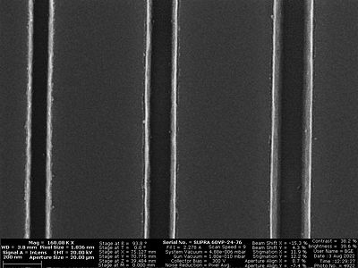
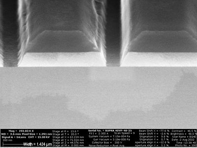
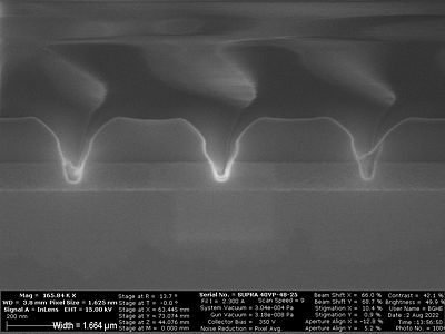
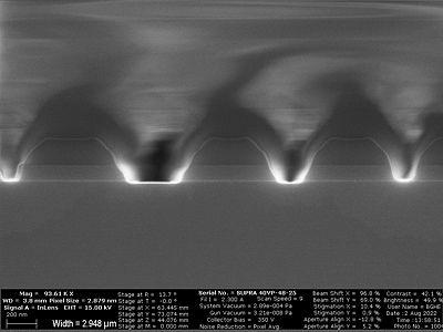
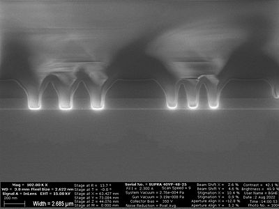
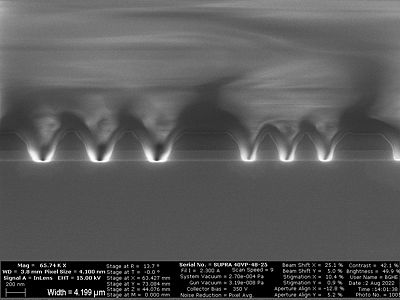
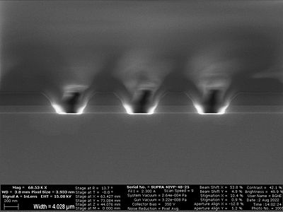
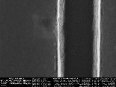
<gallery caption="Profile view, etch time 40 min, started with 380 nm zep resist" widths="400px" heights="325px" perrow="3"> | |||
Image:S038116_01.jpg | |||
Image:S038116_12.jpg | |||
Image:S038116_14.jpg | |||
Image:S038116_16.jpg | |||
Image:S038116_17.jpg | |||
Image:S038116_18.jpg | |||
</gallery> | |||
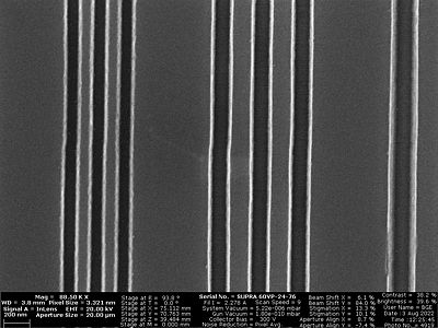
<gallery caption="Top view after resist strip" widths="400px" heights="325px" perrow="3"> | |||
Image:metalS038116top_03.jpg | |||
Image:metalS038116top_04.jpg | |||
Image:metalS038116top_06.jpg | |||
</gallery> | |||
Latest revision as of 13:48, 14 May 2024
Feedback to this page: click here
Al2O3 etching with the ICP metal
| Parameter | Recipe name: Al2O3 Etch |
|---|---|
| Coil Power [W] | 1200 |
| Platen Power [W] | 200 |
| Platen temperature [oC] | 0 |
| BCl3 flow [sccm] | 60 |
| Cl2 flow [sccm] | 30 |
| Pressure [mTorr] | 4 |
| Material to be etched | Etch rate using the above parameters |
|---|---|
| Al2O3 |
|
Al2O3 etching by Sanjeev Vishal Kota sanvis@nanolab
| Parameter | Nanoscale Al2O3 etch | Microscale Al2O3 etch |
|---|---|---|
| Coil Power [W] | 300 | 500 |
| Platen Power [W] | 15 | 70 |
| Platen temperature [oC] | 0 | 0 |
| BCl3 flow [sccm] | 20 | 40 |
| Cl2 flow [sccm] | 7 | 15 |
| Pressure [mTorr] | 1.2 | 3.0 |
| Material to be etched | Nanoscale Al2O3 etch | Microscale Al2O3 etch |
|---|---|---|
| Etch rate | 6.25 nm/min on 6" wafer, Summer sanvis@nanolab | 25 nm/min on small samples on Si carrier, Summer 2022 sanvis@nanolab |
Al2O3 etching by bghe@nanolab
Recipes
| Parameter | Recipe 1:Al2O3 etch platen only |
|---|---|
| BCl3 (sccm) | 15 |
| Ar (sccm) | 15 |
| Pressure (mTorr) | 5 |
| Coil power (W) | 0 |
| Platen power (W) | 30 |
| Temperature (oC) | 20 |
| Spacers (mm) | 100 mm |
Results
- Profile view, etch time 40 min, started with 380 nm zep resist
-
-
-
-
-
-


- Top view after resist strip
-
-
-