Specific Process Knowledge/Lithography/Strip: Difference between revisions
| (19 intermediate revisions by 3 users not shown) | |||
| Line 1: | Line 1: | ||
{{cc-nanolab}} | |||
[[Category: Equipment |Lithography strip]] | '''Feedback to this page''': '''[mailto:labadviser@nanolab.dtu.dk?Subject=Feed%20back%20from%20page%20http://labadviser.nanolab.dtu.dk/index.php?title=Specific_Process_Knowledge/Lithography/Strip click here]''' | ||
[[Category: Equipment|Lithography strip]] | |||
[[Category: Lithography|Strip]] | [[Category: Lithography|Strip]] | ||
__TOC__ | |||
= Strip Comparison Table = | = Strip Comparison Table = | ||
{| border=" | {|border="1" cellspacing="1" cellpadding="10" style="text-align:left;" | ||
!colspan="2" border="none" style="background:silver; color:black;" align="center"|Equipment | !colspan="2" border="none" style="background:silver; color:black;" align="center"|Equipment | ||
|style="background:WhiteSmoke; color:black"|<b>[[Specific_Process_Knowledge/Lithography/Strip# | |style="background:WhiteSmoke; color:black"|<b>[[Specific_Process_Knowledge/Lithography/Strip#Plasma_Asher_1|Plasma Asher 1]]</b> | ||
|style="background:WhiteSmoke; color:black"|<b>[[Specific_Process_Knowledge/Lithography/Strip#Plasma Asher 2|Plasma Asher 2]]</b> | |style="background:WhiteSmoke; color:black"|<b>[[Specific_Process_Knowledge/Lithography/Strip#Plasma Asher 2|Plasma Asher 2]]</b> | ||
|style="background:WhiteSmoke; color:black"|<b>[[Specific_Process_Knowledge/Lithography/Strip#Plasma Asher 3: Descum|Plasma Asher 3: Descum]]</b> | |style="background:WhiteSmoke; color:black"|<b>[[Specific_Process_Knowledge/Lithography/Strip#Plasma Asher 3: Descum|Plasma Asher 3: Descum]]</b> | ||
| Line 133: | Line 137: | ||
<br clear="all" /> | <br clear="all" /> | ||
= Plasma | = Plasma Ashing = | ||
{|border="1" cellspacing="1" cellpadding="10" style="text-align:left;" | |||
|- | |||
|-style="background:silver; color:black" | |||
| | |||
! Photoresist stripping | ! Photoresist stripping | ||
! [[Specific_Process_Knowledge/Lithography/Descum|Descum after lithography]] | ! [[Specific_Process_Knowledge/Lithography/Descum|Descum after lithography]] | ||
| Line 143: | Line 149: | ||
! Ashing of organic material | ! Ashing of organic material | ||
|- | |- | ||
| | |||
|-style="background:whitesmoke; color:black" | |||
!Process pressure | |||
|0.8- 1.2mbar | |0.8- 1.2mbar | ||
|0.5- 1.0mbar | |0.5- 1.0mbar | ||
| Line 149: | Line 157: | ||
|0.8-1.5mbar | |0.8-1.5mbar | ||
|- | |- | ||
| | |||
|-style="background:silver; color:black" | |||
!Process gases | |||
| | | | ||
*O<sub>2</sub> (400 sccm) | *O<sub>2</sub> (400 sccm) | ||
| Line 159: | Line 169: | ||
|O<sub>2</sub> | |O<sub>2</sub> | ||
|- | |- | ||
| | |||
|-style="background:whitesmoke; color:black" | |||
!Process power | |||
|600-1000W | |600-1000W | ||
|150-300W | |150-300W | ||
| Line 165: | Line 177: | ||
|1000W or less for heat- sensitive materials | |1000W or less for heat- sensitive materials | ||
|- | |- | ||
| | |||
|-style="background:silver; color:black" | |||
!Process time | |||
|5-60 minutes | |5-60 minutes | ||
|1-5 minutes | |1-5 minutes | ||
| Line 171: | Line 185: | ||
|Between 0.5 and 20 hours, depending on the material | |Between 0.5 and 20 hours, depending on the material | ||
|- | |- | ||
| | |||
|-style="background:whitesmoke; color:black" | |||
!Batch size | |||
|1-30 | |1-30 | ||
|1-10 | |1-10 | ||
| Line 181: | Line 197: | ||
<br clear="all" /> | <br clear="all" /> | ||
Typical process time for stripping in plasma asher 1 or 2: | |||
*1.5 µm AZ 5214E resist film: ~15 min | |||
*10 µm AZ 4562 resist film: ~45 min | |||
==Plasma | Typical process parameters: | ||
*O<sub>2</sub>: 400 ml/min | |||
*N<sub>2</sub>: 70 ml/min | |||
*Power: 1000 W | |||
A typical descum process in plasma asher 1 or 2: | |||
*O<sub>2</sub>: 70 ml/min | |||
*N<sub>2</sub>: 70 ml/min | |||
*Power: 150 W | |||
*Time : 10 min | |||
Be sure to wait for chamber to cool down to room temperature, before runinng descum processes in plasma asher 1 or 2. At a load of 2 Fused silica wafers, the amount of resist removed will be 10 - 1500 nm. | |||
'''NB: Use dedicated descum asher Plasma Asher 3: Descum for descumming.''' | |||
==Plasma Asher 1== | |||
[[Image:plasmaasher2.JPG|300x300px|thumb|The Plasma Asher 1 is placed in C-1]] | [[Image:plasmaasher2.JPG|300x300px|thumb|The Plasma Asher 1 is placed in C-1]] | ||
The Plasma Asher 1 (TePla 300 auto load model) can be used for the following process: | The Plasma Asher 1 (TePla 300 auto load model) can be used for the following process: | ||
| Line 206: | Line 237: | ||
The machine can be used for almost every materials, but if you have any doubt about your materials are compatible with the plasma process it is better to ask photolithography group at Nanolab. | The machine can be used for almost every materials, but if you have any doubt about your materials are compatible with the plasma process it is better to ask photolithography group at Nanolab. | ||
The user manual, user APV, and contact information can be found in [http://labmanager.dtu.dk/function.php?module=Machine&view=view&mach=55 LabManager] - '''requires login''' | |||
===Process Information=== | ===Process Information=== | ||
| Line 214: | Line 245: | ||
==Plasma Asher 2== | ==Plasma Asher 2== | ||
[[Image:Plasma_Asher_6inch.jpg|300x300px|thumb|Plasma asher for removing AZ resist on 6" wafers: positioned in E-5]] | [[Image:Plasma_Asher_6inch.jpg|300x300px|thumb|Plasma asher for removing AZ resist on 6" wafers: positioned in E-5]] | ||
The Plasma Asher 2 is the same as Plasma Asher 1 but has another loading system which is more convenient for batch loading of 6inch substrates. | The Plasma Asher 2 is the same as Plasma Asher 1 but has another loading system which is more convenient for batch loading of 6inch substrates. | ||
| Line 240: | Line 269: | ||
The other materials have not been tested yet. | The other materials have not been tested yet. | ||
The user manual, user APV, and contact information can be found in [http://labmanager.dtu.dk/function.php?module=Machine&view=view&mach=200 LabManager] - '''requires login''' | |||
===Process Information=== | ===Process Information=== | ||
| Line 250: | Line 279: | ||
==III-V Plasma Asher== | ==III-V Plasma Asher== | ||
[[Image:III-V_asher.jpg|300x300px|thumb|Plasma asher for removing resist on III-V samples: positioned in A-5]] | [[Image:III-V_asher.jpg|300x300px|thumb|Plasma asher for removing resist on III-V samples: positioned in A-5]] | ||
Diener Pico Plasma Asher for III-V materials. | Diener Pico Plasma Asher for III-V materials. | ||
The user manual and contact information can be found in [http://labmanager.dtu.dk/function.php?module=Machine&view=view&mach=186 LabManager] - '''requires login''' | |||
<br clear="all" /> | <br clear="all" /> | ||
--> | --> | ||
==Plasma Asher 3: Descum== | ==Plasma Asher 3: Descum== | ||
[[image:2017-03-15 13.12.45.jpg|350x350px|thumb|Plasma Asher 3: Descum is placed A-5]] | [[image:2017-03-15 13.12.45.jpg|350x350px|thumb|Plasma Asher 3: Descum is placed A-5]] | ||
The Plasma Asher 3: Descum dedicated for resist descum i.e. removal of remains resist traces after development. It has a small chamber, so you can only load one 4 inch substrate ad time or few smaller pieces. | The Plasma Asher 3: Descum dedicated for resist descum i.e. removal of remains resist traces after development. It has a small chamber, so you can only load one 4 inch substrate ad time or few smaller pieces. | ||
| Line 278: | Line 304: | ||
The other materials have not been tested yet. | The other materials have not been tested yet. | ||
The user manual, user APV, and contact information can be found in [http://labmanager.dtu.dk/function.php?module=Machine&view=view&mach=423 LabManager] - '''requires login''' | |||
===Process Information=== | ===Process Information=== | ||
| Line 288: | Line 314: | ||
==III-V Plasma Asher== | ==III-V Plasma Asher== | ||
[[Image:III-V_asher.jpg|300x300px|thumb|Plasma asher for removing resist on III-V samples: positioned in A-5]] | [[Image:III-V_asher.jpg|300x300px|thumb|Plasma asher for removing resist on III-V samples: positioned in A-5]] | ||
Diener Pico Plasma Asher for III-V materials. | Diener Pico Plasma Asher for III-V materials. | ||
The user manual and contact information can be found in [http://labmanager.dtu.dk/function.php?module=Machine&view=view&mach=186 LabManager] - '''requires login''' | |||
<br clear="all" /> | <br clear="all" /> | ||
| Line 299: | Line 323: | ||
=Resist Strip= | =Resist Strip= | ||
[[Image:Resist_strip.jpg|300x300px|thumb|Resist strip bench in D-3]] | |||
[[Image:Resist_strip.jpg|300x300px|thumb| | |||
This resist strip is only for wafers without metal and SU-8. | This resist strip is only for wafers without metal and SU-8. | ||
| Line 314: | Line 335: | ||
The user manual and contact information can be found in LabManager: [http://labmanager.dtu.dk/function.php?module=Machine&view=view&mach=385 Resist Strip] - '''requires login''' | |||
<br clear="all" /> | <br clear="all" /> | ||
| Line 320: | Line 341: | ||
==Overview of wet bench 06 and 07== | ==Overview of wet bench 06 and 07== | ||
{| border=" | {|border="1" cellspacing="1" cellpadding="10" style="text-align:left;" | ||
|-style="background:silver; color:black" | |||
| | |||
! [[Specific Process Knowledge/Lithography/Strip#Resist_Strip|Resist Strip]] | ! [[Specific Process Knowledge/Lithography/Strip#Resist_Strip|Resist Strip]] | ||
! [[Specific Process Knowledge/Lithography/LiftOff#Lift-off_wet_bench_07|Lift-off]] | ! [[Specific Process Knowledge/Lithography/LiftOff#Lift-off_wet_bench_07|Lift-off]] | ||
|- | |- | ||
| | |||
| | |-style="background:whitesmoke; color:black" | ||
!General description''' | |||
| | |Wet stripping of resist | ||
|Lift-off process | |||
|- | |- | ||
| | |||
|-style="background:silver; color:black" | |||
!Chemical solution | |||
|NMP Remover 1165 | |NMP Remover 1165 | ||
|NMP Remover 1165 | |NMP Remover 1165 | ||
|- | |- | ||
|-style="background:whitesmoke; color:black" | |||
!Process temperature | |||
|Up to 65°C | |||
|Up to 65°C | |||
|- | |- | ||
| | |-style="background:silver; color:black" | ||
!Batch size | |||
| | | | ||
1 - 25 wafers | 1 - 25 wafers | ||
| Line 348: | Line 374: | ||
1 - 25 wafers | 1 - 25 wafers | ||
|- | |- | ||
| | |||
|-style="background:whitesmoke; color:black" | |||
!Size of substrate | |||
| | | | ||
*100 mm wafers | *100 mm wafers | ||
| Line 356: | Line 384: | ||
*150 mm wafers | *150 mm wafers | ||
|- | |- | ||
| | |||
|-style="background:silver; color:black" | |||
!Allowed materials | |||
| | | | ||
*Silicon | *Silicon | ||
| Line 362: | Line 392: | ||
*Silicon Nitride | *Silicon Nitride | ||
*Silicon Oxynitride | *Silicon Oxynitride | ||
| | | | ||
All metals except Type IV (Pb, Te) | |||
|- | |- | ||
|} | |} | ||
Latest revision as of 10:17, 18 March 2024
The contents on this page, including all images and pictures, was created by DTU Nanolab staff unless otherwise stated.
Feedback to this page: click here
Strip Comparison Table
| Equipment | Plasma Asher 1 | Plasma Asher 2 | Plasma Asher 3: Descum | Resist strip | Lift-off | |
|---|---|---|---|---|---|---|
| Purpose |
All purposes |
Clean wafers only, no metal |
Resist descum |
Resist strip, no metal lift off |
Lift-off | |
| Method |
Plasma ashing |
Plasma ashing |
Plasma ashing |
Solvent and ultra sound |
Solvent and ultra sound | |
| Process parameters | Process gasses |
|
|
|
|
|
| Max. process power |
|
|
|
|
| |
| Solvent |
|
|
|
|
| |
| Substrates | Batch size |
|
|
|
|
|
| Allowed materials |
|
No metal allowed!
|
|
No metal allowed!
|
| |
Plasma Ashing
| Photoresist stripping | Descum after lithography | Surface treatment of plastic, ceramic and metal | Ashing of organic material | |
|---|---|---|---|---|
| Process pressure | 0.8- 1.2mbar | 0.5- 1.0mbar | 0.5- 1.0mbar | 0.8-1.5mbar |
| Process gases |
|
|
O2, CF4, N2 or their mixtures | O2 |
| Process power | 600-1000W | 150-300W | 150-300W | 1000W or less for heat- sensitive materials |
| Process time | 5-60 minutes | 1-5 minutes | a few seconds to a few minutes | Between 0.5 and 20 hours, depending on the material |
| Batch size | 1-30 | 1-10 | 1 wafer at a time | 1 wafer at a time, use a container, e.g Petri dish |
Typical process time for stripping in plasma asher 1 or 2:
- 1.5 µm AZ 5214E resist film: ~15 min
- 10 µm AZ 4562 resist film: ~45 min
Typical process parameters:
- O2: 400 ml/min
- N2: 70 ml/min
- Power: 1000 W
A typical descum process in plasma asher 1 or 2:
- O2: 70 ml/min
- N2: 70 ml/min
- Power: 150 W
- Time : 10 min
Be sure to wait for chamber to cool down to room temperature, before runinng descum processes in plasma asher 1 or 2. At a load of 2 Fused silica wafers, the amount of resist removed will be 10 - 1500 nm.
NB: Use dedicated descum asher Plasma Asher 3: Descum for descumming.
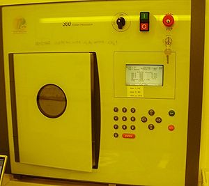
Plasma Asher 1

The Plasma Asher 1 (TePla 300 auto load model) can be used for the following process:
- Photoresist stripping
- Descumming
- Surface cleaning after storage
- Surface cleaning after processes using oil pump or diffusion pump vacuum
- Surface cleaning as part of photolithography after wet developing of lacquer structures prior to wet or plasma etching
- Stripping of photoresist layers after etching, including after being exposed to high temperatures as after implantation, ion etching, sputter etching, RIE
- Removal of organic passivation layers and masks
- Etching of glass and ceramic
- Etching of SiO, SiN, Si
- Removal of polyimide layers
The machine can be used for almost every materials, but if you have any doubt about your materials are compatible with the plasma process it is better to ask photolithography group at Nanolab.
The user manual, user APV, and contact information can be found in LabManager - requires login
Process Information
Plasma Asher 2

The Plasma Asher 2 is the same as Plasma Asher 1 but has another loading system which is more convenient for batch loading of 6inch substrates.
In this machine, only O2 and N2 gases are used for processes (in PlasmaAsher1, CF4 is used as well).
The typical process parameters when operating the equipment:
- Photeresist stripping
Pressure: 0.8 - 1.0 mbar
Gas: O2
Power: 600 - 1000 watts
Time: 5 -30 min., depending on photoresist type and thickness
A typical process time for stripping of 1.5 um AZ5214e resist is 25 min for 6 wafers load in a boat, recipe 18.
A Descum process in manual mode: O2:70, N2:70, power:150W, time:10 min
Be sure to wait for cooling if the mashine has been used at 1000W right before. At a load at 2 Fused silica wafers resist removed 0.01-01,5um
The other materials have not been tested yet.
The user manual, user APV, and contact information can be found in LabManager - requires login
Process Information
Plasma Asher 3: Descum

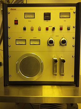
The Plasma Asher 3: Descum dedicated for resist descum i.e. removal of remains resist traces after development. It has a small chamber, so you can only load one 4 inch substrate ad time or few smaller pieces.
In this machine, only O2 and N2 gases are used for processes.
The typical process parameters when operating the equipment:
- Photeresist descum
Pressure: 0.2 - 0.8mbar Gas: O2 Power: 50% - 100% Time: 1 -10 min., depending on photoresist type and thickness
The other materials have not been tested yet.
The user manual, user APV, and contact information can be found in LabManager - requires login
Process Information
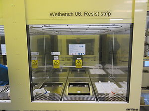
Resist Strip

This resist strip is only for wafers without metal and SU-8.
There are one Remover 1165 bath for stripping and one IPA bath for rinsing.
Here are the main rules for resist strip use:
- Place the wafers in a wafer holder and put them in the first bath for 10 min, this time is depending how much resist you have on the surface.
- After the strip rinse your wafers in the IPA bath for 2-3 min.
- Rinse your wafers for 4-5 min. in running water after stripping.
The user manual and contact information can be found in LabManager: Resist Strip - requires login
Overview of wet bench 06 and 07
| Resist Strip | Lift-off | |
|---|---|---|
| General description | Wet stripping of resist | Lift-off process |
| Chemical solution | NMP Remover 1165 | NMP Remover 1165 |
| Process temperature | Up to 65°C | Up to 65°C |
| Batch size |
1 - 25 wafers |
1 - 25 wafers |
| Size of substrate |
|
|
| Allowed materials |
|
All metals except Type IV (Pb, Te) |


