Specific Process Knowledge/Etch/DRIE-Pegasus/Pegasus-3: Difference between revisions
| (6 intermediate revisions by 2 users not shown) | |||
| Line 7: | Line 7: | ||
==Pegasus 3 - 150mm silicon etching== | ==Pegasus 3 - 150mm silicon etching== | ||
{{Contentbydryetch}} | |||
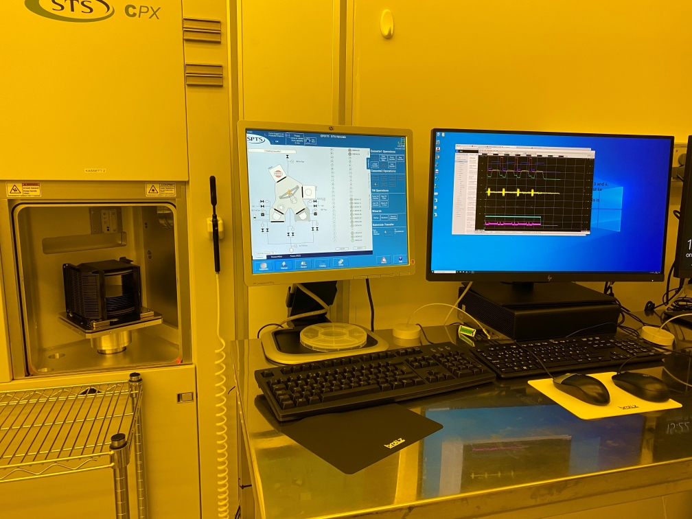
[[Image:05x.jpg |frame|left|x300px|The Pegasus 3 cassette station (left), operator station (center) and support computer with Picoscope process monitoring.{{photo1}} ]] | |||
[[Image:05x.jpg |frame|left|x300px|The Pegasus 3 cassette station (left), operator station (center) and support computer with Picoscope process monitoring. ]] | |||
| Line 25: | Line 19: | ||
'''Standard recipes''' | '''Standard recipes''' | ||
*[[Specific Process Knowledge/Etch/DRIE-Pegasus/Pegasus-3/DREM | The DREM recipes 0.5 kW and 0.2 kW ]] | |||
| Line 53: | Line 46: | ||
<!-- *[[Specific Process Knowledge/Etch/DRIE-Pegasus/VeeryDeeep| Very deep etching]] --> | <!-- *[[Specific Process Knowledge/Etch/DRIE-Pegasus/VeeryDeeep| Very deep etching]] --> | ||
*[[/SiO2 etch|Etch of very thin layers of SiO2]] | |||
=== Wafer bonding === | === Wafer bonding === | ||
Latest revision as of 12:50, 25 January 2024
Feedback to this page: click here
Pegasus 3 - 150mm silicon etching
Unless otherwise stated, the content of this page was created by the dry etch group at DTU Nanolab

The user manual(s) is available, technical information and contact information can be found in LabManager:
Equipment info in LabManager
Process information
Standard recipes
Hardware changes
Compared to a standard SPTS DRIE Pegasus chamber, the Pegasus 3 has had the same modifications as the Pegasus 1 with the exception of the Claritas EPD system. The changes are listed below.
The original (fast switching and with a maximum flow of 1200 sccm) SF6 MFC was causing problems for a long a time so it was replaced by two new MFC's:
- SF6-1: Fast switching MFC for Bosch processes with a maximum flow rate of 600 sccm. It sits in the position of the old 1200 sccm MFC on top of the plasma source.
- SF6-2: Normal MFC for continuous processes with a maximum flow rate of 100 sccm. It is installed in the gas cabinet next to the Ar MFC.
Other etch processes
More processes, such as for DUV resist, are currently being developed, but they are not quite 'ready for publication' at LabAdviser so please contact Jonas (mailto:jmli@dtu.dk) for more information.
Wafer bonding
To find information on how to bond wafers or chips to a carrier wafer, click here.
Internal Nanolab Process log for Pegasus 3
Process log at Nanolab [1]
