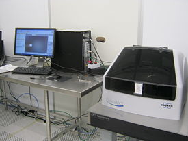
Specific Process Knowledge/Characterization/Dektak XTA
The content on this page, including all images and pictures, was created by DTU Nanolab staff, unless otherwise stated.
Feedback to this page: click here
Dektak XTA (Stylus Profiler)

The Dektak XTA stylus profiler from Brüker is used for profiling surfaces of samples with structures in the micro- and nanometer range. The size of the structures that can be measured is limited by the tip dimensions.
A profile measurement can be done across a specific structure by using a high magnification camera to locate the structure. It is also possible to program the stylus to measure in several positions, defined with respect to some deskew points. Stress measurements of thin films can be done by measuring the wafer bow. However, for predefined measurement programs or stress measurements, we recommend the P17 profiler.
The user manual, quality control procedure and results, technical information and contact information can be found in LabManager.
Information on measurement accuracy and reproducibility for the stylus profilers may be found here.
Performance and Process Parameters
| Purpose | Profiler for measuring micro structures |
|
|---|---|---|
| Performance | Scan range x y |
|
| Scan range z |
50 Å to 1 mm | |
| Resolution x y |
Down to 0.003 µm theoretically, in practice limited by tip radius | |
| Resolution z |
1 Å, 10 Å, 80 Å or 160 Å for ranges 65 kÅ, 655 kÅ, 5240 kÅ and 1 mm respectively | |
| Height accuracy z (95 % confidence) |
| |
| Max scan depth as a function of trench width W |
1.2*(W[µm]-5µm) | |
| Hardware settings | Tip radius |
|
| Substrates and films | Substrate size |
|
| Materials allowed |
|
