Specific Process Knowledge/Thin film deposition/Deposition of Silicon Oxide/Deposition of Silicon Oxide using LPCVD TEOS
Danchip have one LPCVD furnace for deposition of TEOS: The furnace was installed in 1995 and can handle 4" wafers. It is furthermore possible to dope the TEOS with either Boron or phosphorous.


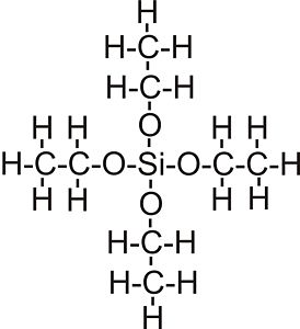
TEOS is Tetra-Ethyl-Ortho-Silicate, it is also sometimes referred to as Tetra-Ethoxy-Silane. The difference between TEOS and Silane is essentially that is TEOS the silicon atom is already oxidised. Therefore the conversion of TEOS to Silicon dioxide is a rearrangement rather than an oxidation. As can be seen from figure 1 what is basically required to deposit Silicon dioxide is a removal of two oxygen atoms for that a relative high temperature of 725 degrees C.
On the new LPCVD TEOS furnace there are two standard processes for deposition, one for thin oxides called TEOSPNE and one for thicker oxides called TEOSSLOW. The only difference is that in the case of the TEOSSLOW recipe the furnace opens significantly slower. Thick TEOS layers have a tendency to form cracks if they are moved to fast out of the furnace.
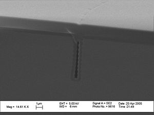
TEOS can be used as an alternative to thermally grown or PECVD oxide, it has a dielectric constant of 3.56 (For thermal oxide it is 3.46). Furthermore TEOS has a very high surface mobility enabling it to fill holes that has a large aspect ratio and leaving the surface quite smooth see figure 2, hence it also covers corners and side walls very well.
Process parameters for the two standard deposition recipes on the TEOS furnace:
| Recipe name | Wafer size and number of wafers | Temperature [oC] | Pressure [mTorr] | TEOS gas flow [sccm] | O gas flow [sccm] | PH gas flow [sccm] | TMB gas flow [sccm] | Comments |
|---|---|---|---|---|---|---|---|---|
| "TEOSPNE" | 4" wafers
1-17 wafers in a run |
725 | 190 | 50 | 30 | 0 | 0 | standard TEOS recipe |
| "TEOSSLOW" | 4" wafers
1-17 wafers in a run |
725 | 190 | 50 | 30 | 0 | 0 | Recipe used for thick layers |
Deposition rate:
The deposition rate is normally a little over 10nm/min (10.5nm/min) and the refractive index is around 4.44 for both recipes.
Using LPCVD silicon nitride as a masking material for KOH etching
At Danchip stoichiometric silicon nitride is mainly used as masking material for potassium hydroxide (KOH) etching. The etch rate of the nitride in 80 oC KOH is expected to be less than 1 Å/min.
There are regularly users having problems with pinholes in the silicon nitride after KOH etching. It is not always clear what the reasons are, but we suspect problems can arise due to
- too many or too large particles in the nitride.
- too rough handling of the wafers after the nitride deposition.
- too much stress between the nitride and the underlying layer.
Our recommendations to try and avoid pinhole problems are:
To avoid too many or too large particles in the nitride<br\>
- Use the new nitride furnace, if you have to deposit stoichiometric nitride. In order to avoid problems with particles it is not allowed to deposit low stress nitride in this furnace, and the particles level is therefore low compared to the older nitride furnace
- Before running a process keep in close contact with the Danchip staff (especially the process specialist on the furnace) or take a look at the logbook to make sure that the nitride furnace is expected to be in a good state.
To avoid too rough handling of the wafers after the nitride deposition<br\>
- After the deposition handle the wafers with a clean glove on the edge of the wafers (no tweezers).
- Be careful not to scratch wafers with nitride (e.g. up against each other or on the spinner or the aligner).
- If you have nitride on the back side of a wafer while aligning, consider if you can protect it with e.g. a photoresist layer before loading it onto the aligner. Or use a non-vacuum aligner chuck with a big hole in the middle, so that the wafer is only laying on the edge. Avoid hard contact in the aligner if possible.
To avoid too much stress between the nitride and the underlying layer<br\>
- It is recommended to have a of silicon oxide layer between the silicon substrate and the nitride layer to reduce the stress level between the layers. The silicon nitride is then expected to have less tendency to break.
for sjov
Failed to parse (unknown function "\includegraphics"): {\displaystyle \includegraphics[width=0.5\textwidth]{RIE1_Si_Angle_O2_CHF3.jpg} \caption{The simplified model, which can be used in stead of the one in figure. In this representation is the total resistance in the entire transmission lines, not just between the capacitors.} }
