Aligner: Maskless 03
 Aligner: Maskless 03 is located in E-5.
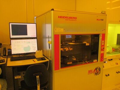
MLA150 WMII maskless aligner from Heidelberg Instruments GmbH, installed 2020.
Special features:
- Backside Alignment
- Advanced Field Alignment Mode for alignment to individual chips/devices on the substrate
- Separate conversion PC (Power PC)
Link to information about alignment mark design.
Training videos
Equipment info in LabManager - requires login
Exposure dose and defocus
Information on UV exposure dose
Quality Control (QC)
| Quality Control (QC) for Aligner: Maskless 03 (MLA3) - Dose and Defoc
|
| QC Recipe:
|
Dose and defocus test on 1.5µm AZ5214E
|
| Dose test
|
Last QC value ± 20 mJ/cm2 (9 steps total)
|
| Defoc test
|
Last QC value ± 8 (9 steps total)
|
|
| QC limits
|
Aligner: Maskless 03 (MLA3)
|
| Dose
|
none
|
| Defoc
|
none
|
|
Dose and defoc values are reported in the QC data sheet.
|
| Quality Control (QC) for Aligner: Maskless 03 (MLA3) - Alignment
|
| QC Recipe:
|
Alignment accuracy test
|
| Topside alignment
|
Expose an overlay design after automatic alignment to 4 alignment marks using the High Res camera and applying scaling and shearing.
Alignment accuracy in 9 points across a 100mm wafer is measured, the average alignment error is reported.
|
| Backside alignment
|
Expose an overlay design after automatic alignment to 4 backside alignment marks and applying scaling and shearing. Rotate the wafer 180° and repeat.
Alignment accuracy in 9 points across a 100mm wafer is measured, half the average alignment error is reported.
|
|
| QC limits
|
Aligner: Maskless 03 (MLA3)
|
| Topside alignment error
|
>0.5µm
|
| Backside alignment error
|
>1µm
|
|
Camera offsets will be adjusted if alignment error is outside the limit.
|
Equipment performance and process related parameters
| Purpose
|
|
Alignment and UV exposure
|
| Performance
|
Exposure mode
|
Projection
|
| Exposure light
|
405nm
(laser diode array)
|
| Focusing method
|
Pneumatic
|
| Minimum structure size
|
down to 1 µm
|
| Design formats
|
- GDS-II
- CIF
- DXF
- Gerber
- HIMT format
|
| Alignment modes
|
- Top side alignment, ±0.5µm
- Backside alignment, ±1.0µm
- Field alignment (chip-by-chip TSA), ±0.25µm (within 5x5mm2 area)
|
| Substrates
|
Substrate size
|
- maximum writing area: 150x150 mm2
- 150 mm wafer
- 100 mm wafer
- 50 mm wafer
- pieces down to 5x5 mm2
|
| Allowed materials
|
All cleanroom materials
Total height variation across the substrate must be less than ±90 µm - including wafer bow
|
| Batch
|
1
|
