Specific Process Knowledge/Thin film deposition/Furnace LPCVD PolySilicon/Boron doped poly-Si
Results from the acceptance test 2012
| Recipe name | Deposition rate [nm/min] | Refractive index@630nm | Thickness variation on center wafer | Thickness variation along the boat | Surface roughness [nm] | Sheet resistance [Ohms/square] | Boron concentation [boron atoms/cm3] | Comments |
|---|---|---|---|---|---|---|---|---|
| "DOPEPOLY" | ~ 4.0-4.1 (4" wafers) |
1.29%-1.38% (4" wafers) |
1.63%-1.81% (4" wafers) |
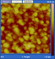
~ 4.83, measured with AFM standard tip (273 nm layer) |
157-171, variation over boat 4.5% (4" wafers) |
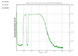
~ 1021 boron atoms/cm3. "Dopepoly" recipe, 30 minutes deposition, Poly-Si thickness is ~104nm, Aug. 2014. | Run-to-run uniformity: 1.43 % (4" wafers, 3 runs) |
Results from Tempress test January 2023 - New standard parameters
In January 2023 Tempress optimized the process for boron doped polysilicon again.
Tempress made a number of depositions in the furnace. All depositions were done with 25 wafers in the furnace, and only 6" wafers were used. On each side of the wafers, a boat with ten 6" dummy wafers was placed.
The process parameters and the injector design that Tempress came up with will replace the old "DOPEPOLY" recipe from the acceptance test.
The results in the table below are the best process parameters that were found (from run number 10. If you want some information about other runs/other process parameters that were tested, then contact the Thin Film group).
After the depositions of boron doped polysilicon, undoped polysilicon was deposited one some test wafers for two times 30 minutes. No sheet resistance could be measured on the wafers, and it is therefore assumed that they were not affected by the doping.
| Recipe name | Number of wafers and wafer size | Temperature [oC] (zone 1, 2, 3, 4, 5) | Gas flows [sccm] | Pressure [mTorr] | Deposition rate [nm/min] | Deposition rate - Uniformity over one wafer [%] | Deposition rate - Uniformity over the boat [%] | Sheet resistance [Ohms/square] | Sheet resistance - Uniformity over one wafer [%] | Sheet resistance - Uniformity over the boat [%] |
|---|---|---|---|---|---|---|---|---|---|---|
| "POLYBOR" | 25 wafers,
6" wafers |
600, 596, 597, 600, 600 | SiH4 (through injector): 50
BCl3 (through injector): 2 |
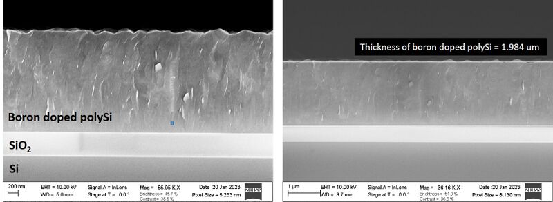
150 | ~ 4.15 (6" wafers) | 2.9 (door side)
1.3 (pump side) |
0.5 | 9.4 (door side)
10.01 (pump side) |
1.6 (door side)
2.0 (pump side) |
3.6 |
Important notes about deposition of boron doped polysilicon
BCl3 (boron trichloride) gas is used for the boron doping. This is introduced into the furnace through an injector together with SiH4 (silane) gas.
The injector is a long, thin quartz tube with eight 0.7 mm wide holes, and this is needed to be able to distribute a very small flow of 2 sccm BCl3 gas over the wafers in the furnace.
A new injector design was invented for the process. This design is called "8010000256 injector trial 1 0.7mm x8holes" (contact the Thin Film group, if you need more information). The injector has to be mounted in the furnace with the holes pointing towards "10 o'clock", and this can be done without cooling down the furnace - but absolute only by a service technician.
An injector can only be used for a limited number of depositions, because it will be covered with polysilicon which has another stress level than the quartz. When about 10 μm of polysilicon has been deposited on the injector, it might break. This actually happened during the testing - The injector exploded and left a very high number of quartz and polysilicon pieces inside the furnace tube and on the cantilever.
Furthermore, the injector should only be mounted in the furnace, when boron doped polysilicon is being deposited, otherwise the holes in the injector will be blocked. For deposition of undoped polysilicon and amorphous silicon, only SiH4 gas in being used, and this in introduced directly into the furnace at the door, not through the injector.
January 2023: DTU Nanolab only has one injector that was used to optimize the process for boron doped polysilicon, and this can only be used for a limited number of depositions. Some new injectors will therefore have to be ordered, before a standard process for deposition of boron doped polysilicon will be available on the furnace.


