Specific Process Knowledge/Thin film deposition/Deposition of polysilicon/Deposition of polysilicon using LPCVD/Standard recipes, QC limits and results for the 6" polysilicon furnace
Feedback to this page: click here
Unless otherwise stated, this page is written by DTU Nanolab internal
Standard recipes on the 6" polysilicon furnace (this recipe is being watched in the in the quality assurance program):
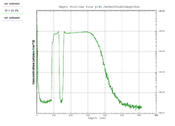
| Quality Controle (QC) for the 6" LPCVD polysilicon furnace | |||||||||||||||||||||||||||||
| |||||||||||||||||||||||||||||
Expected results when using the standard recipes on the 6" polysilicon furnace:
| QC Recipe | Polysilicon deposition
rate [nm/min] |
Standard deviation for the
polysilicon deposition rate [%] |
Refractive index | Standard deviation for the
refractive index [%] | |
|---|---|---|---|---|---|
| Over the center wafer
4" wafers
|
"POLY" | 7.99 | 0.68 | 3.95 | 0.04 |
| Over the boat
4" wafers
|
"POLY" | 7.87 | 0.67 | 3.95 | 0.05 |
| Over the center wafer
6" wafers
|
"POLY" | 7.21 | 0.57 | 3.96 | 0.02 |
| Over the boat
6" wafers
|
"POLY" | 7.19 | 0.52 | 3.96 | 0.03 |
Process parameters for the standard recipes on the 6" LPCVD polySi furnaces:
| Recipe name | Wafer size and number of wafers | polySi thickness [nm] | Temperature [oC] | Pressure [mTorr] | SiH4 gas flow [sccm] | BCl3 gas flow [sccm] | Comments |
|---|---|---|---|---|---|---|---|
| "POLY" | 4" or 6" wafers
1-25 wafers |
0 - 2000 | 616-625 | 200 | 70 | 0 | |
| "DOPDPOLY" | 4" or 6" wafers
1-25 wafers |
0 - 1000 |
596-600 |
150 | 50 | 1 | Boron doping not available at the moment |
| "AMORPH" | 4" or 6" wafers
1-25 wafers |
0 - 2000 | 562-565 | 200 | 70 | 0 | |
| "DOPEAMOR" | 4" or 6" wafers
1-25 wafers |
0 - 2000 | 556-565 | 150 | 50 | 1 | Boron doping not available at the moment |
Expected results when using the standard recipe on the 6" LPCVD polySi furnace:
These are typical values
| Recipe name | Deposition rate [nm/min] | Refractive index@630nm | Thickness variation on center wafer | Thickness variation along the boat | Surface roughness [nm] | Sheet resistance [Ohms/square] | Boron concentation [boron atoms/cm3] | Comments |
|---|---|---|---|---|---|---|---|---|
| "POLY" | ~ 8-9 (4" wafers) | ~ 3.9 | < 2% | < 4% | ~ 5.66, measured with AFM standard tip (244 nm layer) | See quality control data for latest measurements.
Standard polySi not part of the acceptance test. | ||
| "DOPEPOLY" | ~ 4.0-4.1 (4" wafers) | < 2%
Acceptance test March 2012: 1.29%-1.38% (4" wafers) |
< 4%
Acceptance test March 2012: 1.63%-1.81% (4" wafers) |
~ 4.83, measured with AFM standard tip (273 nm layer) | ~155-175
Acceptance test March 2012: 157-171, variation over boat 4.5% (4" wafers) |
~ 1021 boron atoms/cm3. "Dopepoly" recipe, 30 minutes deposition, Poly-Si thickness is ~104nm, Aug. 2014. | Run-to-run uniformity, acceptance test March 2012: 1.43 % (4" wafers, 3 runs) | |
| "AMORH" | ~ 2.2-2.3 (4" wafers) | ~ 4.54
(see below) |
< 2%
Acceptance test August 2011: 0.80%-1.39% (6" wafers) |
< 4%
Acceptance test August 2011: 0,45%-0.78% (6" wafers) |
~ 0.47, measured with AFM standard tip (134 nm layer) | Run-to-run uniformity, acceptance test August 2011: 0.29 % (6" wafers, 3 runs) |


The deposition rate changes a little over time, but generally it is fairly good from run to run. The last measured values of the polySi thicknesses can be found on the Poly Si page in the 6" Furnace logbook and in the quality control data (only standard polySi).
Amorphous Si measurement
For amorphous LPCVD Si deposited in August 2022 an ellipsometer measurement and a SEM measurement have been made. The amorphous Si was deposited on a 4" wafer with thermal wet SiO2.
For the SEM measurement the wafer was first cleaved, and then the layer thicknesses were measured. As seen from the SEM pictures below, the thickness of the amorphous Si layer was measured to be 895 nm, and the thickness of the SiO2 layer was measured to be 314 nm.

For the ellipsometer measurement, it was tried to measure the thickness and the optical parameters using different models. Below the best measurement result is show and also the refractive index (n) and the extinction coefficient (k) as function of wavelength. The thickness of the amorphous Si layer is measured to be 929.75 nm, and at 632.8 nm wavelenght n is 4.54 and k is 1.18. The thickness of the SiO2 layer is measured to be 314.14 nm.


By comparing the SEM and the ellipsometer measurements, it can be seen that not exactly the same thickness of the amorphous Si layer is measured. This indicates the the optical parameters measured by the ellipsometer might also be a bit off, even though the measurement fits very well to the model.