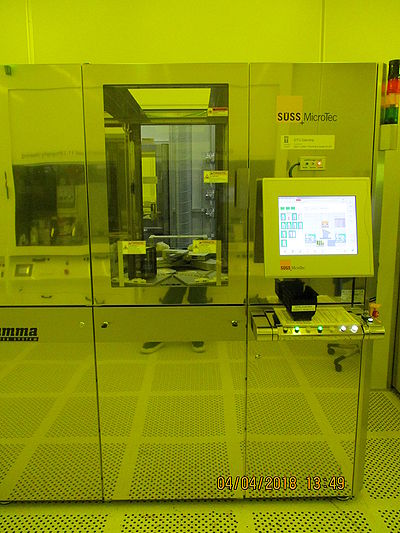
Specific Process Knowledge/Lithography/Coaters/GammaEbeam
Spin Coater: Gamma E-beam and UV
Spin Coater: Gamma E-beam and UV was installed at DTU Nanolab in June 2017. It is a Gamma 4M cluster from Süss MicroTec with spin coating, HMDS vapour priming, and baking modules. The system handles 2", 4", and 6" wafers without size conversion, using two separate coater stations.
The 2" coater station is equipped with 1 resist line, as well as 1 syringe line:
- AR-P 6200.09 (CSAR)
- Syringe, which can be used for various resists (anisole-based or PGMEA-based). We currently recommend against using the syringe, as the process setup is quite demanding. Use a manual spin coater instead.
The 4"/6" coater station is equipped with 4 different resists lines:
- AZ 5214E
- AZ MiR 701
- AR-P 6200.09 (CSAR)
- AZ 4562
The processes that are available on the system are developed by Nanolab. Upon request, it is possible to establish new processes. Use of the syringe requires special training, and requires batch processing - it is not for processing a few wafers now and then.
The user manual, quality control procedures and results, user APVs, and contact information can be found in LabManager - requires login
Process information
| Purpose |
| |
|---|---|---|
| Resist |
| |
| Performance | HMDS contact angle |
60 - 80° (on Silicon) |
| Coating thickness |
| |
| Process parameters | Priming temperature |
120 °C |
| Spin speed |
10 - 6000 rpm | |
| Spin acceleration |
10 - 10000 rpm/s | |
| Hotplate temperature |
25 - 200 °C | |
| Cool plate temperature |
21 °C | |
| Substrates | Substrate size |
|
| Allowed materials |
Silicon, III-V, and glass Resists and crystalbond are not allowed in the HMDS module | |
| Batch |
1 - 25 |
