Specific Process Knowledge/Thin film deposition/Deposition of Copper/Deposition of Copper
Feedback to this page: click here
Roughness of Cu layers
The result here from Katharina Nilson @ nanolab (December 2008 )
The roughness of Cu layers deposited in the Alcate e-beam evaporator was examined by AFM measurements. The Alcatel has been decomissioned, but results may be similar for our current e-beam evaporators, though this has not been verified.
Experimental
Cr was deposited in Alcatel onto Si wafers. (Part of the surface was covered with resist, and a lift-off process followed). The deposition rate was 10 Å/s (the thickness of the layers were between 70 nm and 200 nm). AFM measurements shows the surface structure.
Results
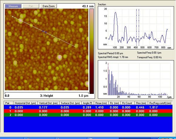
The Cu surface is rather un-uniform and rough. Large grains, randomly distributed, can be seen on the film surface. The largest part of the surface consists of smaller, circular grains, with a diameter of about 25-40 nm. These are seen in the AFM picture with a height of a few nm, as can be observed below. The largest grains are up to 70 nm in diameter, and have a height of up to 20 nm.

AFM picture of a Cu surface deposited in Alcatel. A profile of the surface is shown to the right, where the height of some structures can be seen.
