Specific Process Knowledge/Thin film deposition/ALD2 (PEALD)/TiN deposition using ALD2
Feedback to this page: click here
This page is written by DTU Nanolab internal
General information
As already mentioned in the general ALD2 (PEALD) page, oxides and nitrides cannot be deposited at the same time. Since deposition of aluminum nitride requires the plasma source, and since the highest quality titanium nitride is deposited using plasma, it has been decided to run all nitride deposition processes without the thermal lid. Hence, the chamber volume is larger than with the thermal lid, which causes the substrate temperature to be approximately 50& °C lower than the setpoint.
Result from the acceptance test
Deposition of thermal TiN using TMA and NH3 precursors
Recipe name: "TiN thermal with lid" or "TiN thermal without lid".
| TiCl4 | NH3 | |
|---|---|---|
| Nitrogen flow | 100 sccm | 100 sccm |
| Pulse time | 0.1 s | 2.0 s |
| Purge time | 2.0 s | 6.0 s |
DTU Nanolab performed a deposition with 2000 cycles at 450 °C, where the average growth rate was measured to be 0.0173 nm/cycle.
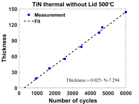
A number of depositions at 500 °C have been made by Evgeniy Shkondin, DTU Photonics (now DTU Nanolab). The number of cycles has been changed, and the thickness as a function of the number of cycles has been plotted as shown in the figure below.
Unlike other ALD materials, the thickness of a deposited TiN layer cannot be measured using the ellipsometer. Hence, one must cleave the wafer and measure its thickness using the SEM. Thin layers (less than 20 nm) are challenging to focus on due to charging and vibrations, making them difficult to measure accurately.
-

TiN cross section of a sample with 2000 cycles deposition at 400 °C on a silicon wafer with thermal oxide. The TiN thickness is 35.8 nm and the SiO2 thickness is 173.8 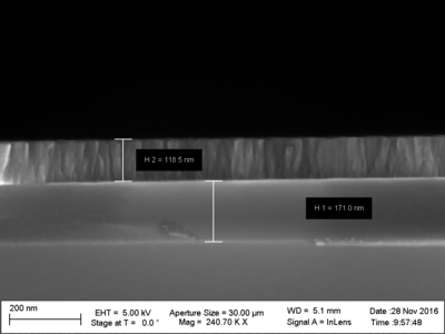
TiN cross section of a sample with 5000 cycles deposition at 400 °C on a silicon wafer with thermal oxide. The TiN thickness is 118.5 nm and the SiO2 thickness is 171.0
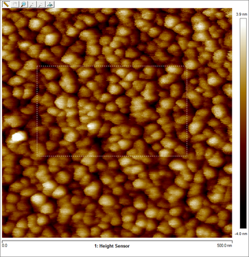
The roughness of TiN deposited at 450 °C has been measured to be 0.7415 nm as shown in the figure below.
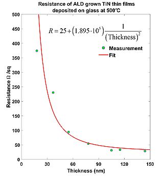
The resistance of the deposited TiN layer strongly depends on the thickness. For very thin layers, a high resistance is measured, and for thicker layers, the resistance decreases. The resistance of TiN deposited on glass at 500 °C as a function of the thickness can be seen in the figure below (Evgeniy Shkondin, DTU Photonics (now DTU Nanolab), May 2017).
Deposition of thermal TiN on trenches using TMA and NH3 precursors
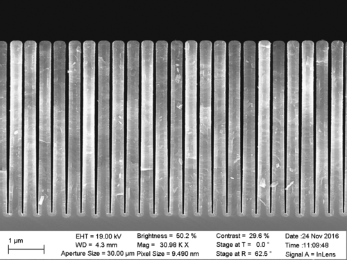
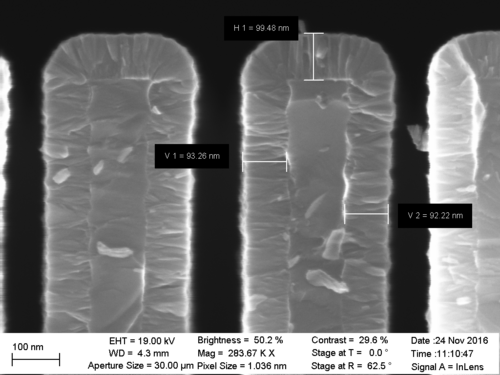
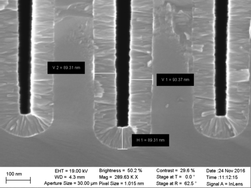
A TiN deposition was done with 4000 cycles at 450 °C, where the average growth rate was measured to be 0.0232 nm/cycle.
| TiCl4 | NH3 | |
|---|---|---|
| Nitrogen flow | 100 sccm | 100 sccm |
| Pulse time | 0.5 s | 5.0 s |
| Purge time | 2.0 s | 6.0 s |
The SEM images below show a homogeneous coverage all over the trenches.
Pernille Voss Larsen, Mikkel Dysseholm Mar and Tanja Amport, DTU Nanolab, 2016-2017.

