Specific Process Knowledge/Etch/III-V ICP/InP-InGaAsP-InGaAs/InP etch with Cl2-H2-Ar
Feedback to this page: click here
The content on this page, including all images and pictures, was created by Berit Herstrøm @ DTU Nanolab (BGHE), unless otherwise stated.
InP etching with Cl2 and H2 including some Ar (Done by bghe@Nanolab)
| Parameter | SiO2 mask before etch | Carrier | Coil power | Platen power | Pressure | Flow rate Cl2 | Flow rate H2 | Flow rate Ar | T | Process time | Comment | Results image1 | Results image2 | Results image3 | CD change | Profile angles | Etch rate in InP | Etch rate in SiO2 | Selectivity (InP:SiO2) |
|---|---|---|---|---|---|---|---|---|---|---|---|---|---|---|---|---|---|---|---|
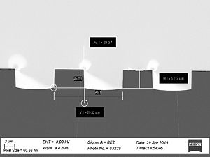
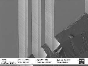
| 20190222 s009209 s12 | 500nm | silicon | 800W | 150 W / 134V | 0.5 mTorr | 6.6 sccm | 5.4 sccm | 0 sccm | 180 | 6:00 min | 
|

|

|
90 |
925nm/min |
54 nm/min |
~17 | ||
| 20190226 s009224 s13 | 500nm | silicon | 800W | 150 W /134V | 1.0 mTorr | 6.6 sccm | 5.4 sccm | 12 sccm | 180 | 4:00 min | 
|

|

|
~95 degrees |
750 nm/min |
58 nm/min |
~13 | ||
| 20190222 s009226 s14 | 500nm | silicon | 1200 W | 150 W /87V | 1.0 mTorr | 6.6 sccm | 5.4 sccm | 12 sccm | 180 | 4:00 min | 
|

|

|
~95 degrees |
790 nm/min |
51 nm/min |
~15.5 | ||
| 20190403 s s15 | 500nm | silicon | 800W | 150 W / 140V | 0.5 mTorr | 6.6 sccm | 5.4 sccm | 0 sccm | 180 | 6:00 min | 
|

|
91.2-92.1 larger on smaller lines |
893-972 nm/min |
52 nm/min |
17-19 | |||
| 20190403 s s16 | 500nm | silicon | 600W | 150 W / 180V | 0.5 mTorr | 6.6 sccm | 5.4 sccm | 0 sccm | 180 | 6:00 min | 
|

|
91.2-92.1 larger on smaller lines |
900-940 nm/min |
53 nm/min |
17-18 | |||
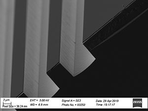
| 20190403 s s17 | 500nm | silicon | 1200W | 150 W/50W 0V | 0.5 mTorr | 6.6 sccm | 5.4 sccm | 0 sccm | 180 | 6:00 min | 
|

|
Undercut |
330 nm/min |
6-7 nm/min |
50 | |||
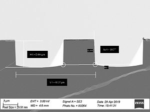
| 20190501 s18 | 500nm | silicon | 1200W | 150 W 110V | 0.6 mTorr | 6.6 sccm | 5.4 sccm | 0 sccm | 180 | 6:00 min | 
|

|
91.5-92.0 |
927 nm/min |
55 nm/min |
17 | |||
| 20190501 s19 | 500nm | silicon | 1200W | 220 W 150V | 0.6 mTorr | 6.6 sccm | 5.4 sccm | 0 sccm | 180 | 6:00 min | Process Failed |
nm/min |
nm/min |
||||||
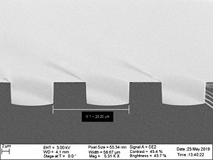
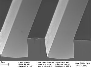
| 20190501 s20 | 500nm | silicon | 1200W | 220 W /150V | 0.6 mTorr | 6.6 sccm | 5.4 sccm | 0 sccm | 180 | 6:10 min | 
|

|
93-94 |
1077 nm/min |
70 nm/min |
15 | |||
| 500nm | silicon | 800W | 150 W / | 1.0 mTorr | 6.6 sccm | 9.4 sccm | 8.0 sccm | 180 | 7:30 min |
degrees |
nm/min |
nm/min |
Variation of coil power only
-
 s15 800W, 870 nm/min
 -
 s16 600W, 907 nm/min
 -
 s18 1200W, 927 nm/min
-
 s15
s15 -
 s16
s16 -
 s18
s18
