Specific Process Knowledge/Etch/ICP Metal Etcher/Chromium/End point
Feedback to this page': click here
Made by Berit bghe @ DTU Nanolab
Using the standard Cr etch recipe I was etching through 100 nm Cr on a 150 mm wafer it an etch load of 50%
I recorded the end point signal and tried three different stopping times to figure out when to stop the etch. I want to find out how I can use the end point signal to get the best etch result; Etch through - also in the small patterns without too much over etch.
I was looking at trenches with sizes ranging from 200 nm to 2 µm in width. The masking materials was negative DUV resist: NUV 2300-0.5 of approximately 500 nm. The process flow can be seen here: File:Process_flow_for_test_wafers xx.pdf
Etch close to optimal
The etch rate is faster near the edge. Therefor the trenches are in general wider at the edges. Here all structures has been etched down to the SiO2 layer and the dimensions are close to being unaffected, especially in the middel. The sidewalls are close to 90 degrees; Sometimes a little positive and sometimes a little negative. To improve more the etch rate should be more uniform over the wafer and the Cr should be with small grain sizes. I stopped 41 s after the end point curve 'SUM_C2' top point on the barc etch and 170 s after the end point curve 'CR_Avg_5208' started to drop on the Cr etch.
| Middel of the wafer | Close to wafer edge |
|---|---|
|
|


End point signal
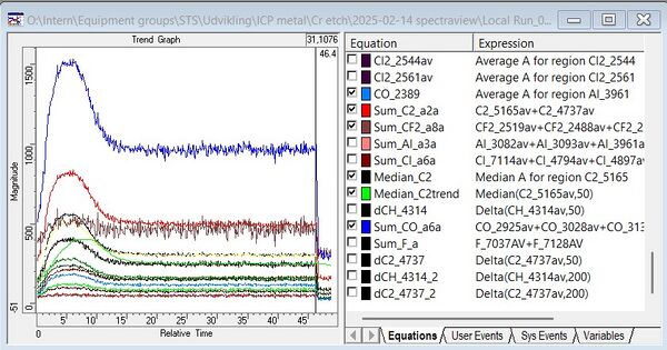
Barc etch
The End point signal shows a top point after 5.5 s and I stopped the etch after 46.4 s giving 41 s after the top point.
- S047676 47s barc etch, Feb-2025, wafer center, 100 nm Cr mask, with 500 nm resist
-

-


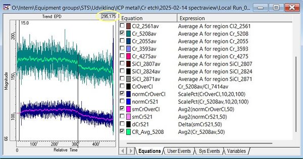
Cr etch
The End point signal shows a drop after 295 s and I stopped the etch after 465 s giving 170 s after the drop started.
- S047676 7:43 min Cr etch, Feb-2025, wafer center, 100 nm Cr mask, with 500 nm resist
-
-


Etched too long
The etch rate is faster near the edge. Therefor the trenches are in general wider at the edges. Here all structures has been etched down to the SiO2 layer but the dimensions are affected, especially at the edge the trenches have become wider. The sidewalls are close to 90 degrees; Sometimes a little positive and sometimes a little negative. The improve more the etch time should be decreased.
| Middel of the wafer | Close to wafer edge |
|---|---|
|
|


End point signal
Barc etch
The End point signal shows a top point after 5.0 s and I stopped the etch after 60 s.
- S047670 60s barc etch, Feb-2025, wafer center, 100 nm Cr mask, with 500 nm resist
-

-


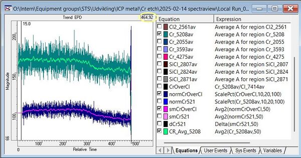
Cr etch
The End point signal shows a drop after 264 s and I stopped the etch after 7:45 min
- S047670 7:45 min Cr etch, Feb-2025, wafer center, 100 nm Cr mask, with 500 nm resist
-

-


Etched too short
The etch rate is faster near the edge. Therefor the trenches are in general wider at the edges. Here all structures has almost been etched down to the SiO2 layer and the dimensions are close to being unaffected. But especially the smallest trenches seems to be not all etched down to the SiO2. Also they are not equally wide. The sidewalls are close to being 90 degrees but some of them seems to have a little foot. To improve more the etch time should be longer - probably especially on the barc etch but maybe also for the Cr etch.
| Middel of the wafer | Close to wafer edge |
|---|---|
|
|


End point signal
Barc etch
The End point signal shows a top point after 6.5 s and I stopped the etch after 30 s. Too short
- S047671 30s barc etch, Feb-2025, wafer center, 100 nm Cr mask, with 500 nm resist
-

-


Cr etch
The End point signal shows a drop after 295 s and I stopped the etch after 7:00 min. Too short
- S047671 7:00 min Cr etch, Feb-2025, wafer center, 100 nm Cr mask, with 500 nm resist
-

-


