| 27/11-2019
|
Medusa One AZ Mir
|
Si / 10%
|
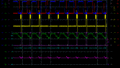
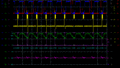
stab-19 TDESC clean5, RF MU runs
|
nanolab/ vy / DREM / DREM 3kW 100% 120 cycles or 10:0 minutes
|
S018605
|
Process log entry
|
|
|
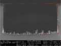
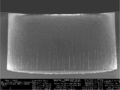
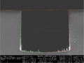
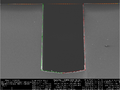
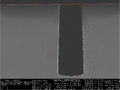
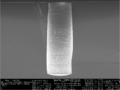
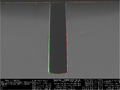
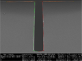
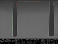
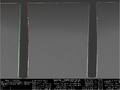
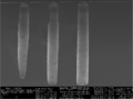
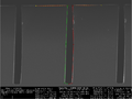
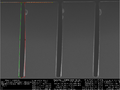
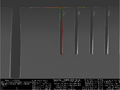
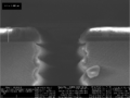
| SEM image:
|
a580
|
a582
|
a583
|
a584
|
a586
|
a587
|
a588
|
a589
|
a591
|
a592
|
a593
|
| Trench width (um) |
250.32 |
160.36 |
80.48 |
40.42 |
25.42 |
16.66 |
10.43 |
8.38 |
5.02 |
2.95 |
3
|
| Etched depth (um) |
144.98 |
143.11 |
138.38 |
126.78 |
116.06 |
105.34 |
93.04 |
87.39 |
76.48 |
65.37 |
62.15
|
| Etch rate (um/min) |
14.5 |
14.31 |
13.84 |
12.68 |
11.61 |
10.53 |
9.3 |
8.74 |
7.65 |
6.54 |
6.22
|
| Etch rate (nm/cyc) |
1.21 |
1.19 |
1.15 |
1.06 |
0.97 |
0.88 |
0.78 |
0.73 |
0.64 |
0.54 |
0.52
|
| Sidewall bowing (%) |
-0.53 |
-0.63 |
-0.12 |
-0.08 |
0.14 |
0.33 |
0.54 |
0.65 |
0.71 |
0.43 |
0.59
|
| Sidewall angle (degs) |
92.18 |
92.25 |
91.6 |
91.51 |
91.32 |
91.19 |
91.02 |
90.92 |
90.88 |
90.99 |
90.48
|
| Bottom bowing (%) |
6.79 |
9.32 |
14.81 |
17.52 |
16.14 |
18.1 |
17.8 |
21.85 |
21.87 |
31.29 |
26.32
|
| Aspect ratio |
0.57 |
0.86 |
1.64 |
2.9 |
4.13 |
5.59 |
7.7 |
8.93 |
12.35 |
16.03 |
17.63
|
|


