Specific Process Knowledge/Etch/AOE (Advanced Oxide Etch)/Quartz etch using AOE
Appearance
Feedback to this page: click here
Nanoetch in quartz 65 mm x 65 mm x 6.25 mm substrates
Unless otherwise stated, all content in this section was done by Berit Herstrøm, DTU Nanolab - the work has been done in august 2011
The tests were done on 2" quartz wafers with a thickness of 1 mm. These were placed on a 65mmx65mmx6,25mm quartz plate with a 2" groove. This 65mmx65mmx6,25mm plate was placed on a 4" Si wafer with a 65mmx65mm groove. the masking material was Cr sputter deposited in Wordentec and and patterned with ZEP520A resist by e-beam and ICP metal Cr etch.
Recipe used QZ65x65:
| Parameter | Recipe name: QZ65x65 |
|---|---|
| Coil Power [W] | 1200 |
| Platen Power [W] | 500 |
| Platen temperature [oC] | 50 |
| CF flow [sccm] | 43 |
| CF flow [sccm] | 20 |
| O flow [sccm] | 10 |
| Pressure [mTorr] | 8 |
| Parameter | Results |
|---|---|
| Etch rate | ~300nm/min |
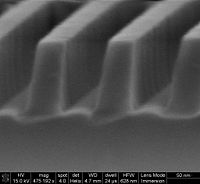
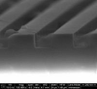
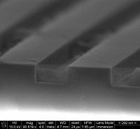
| Etch profile | 86-87 degrees |
| ARDE | There does not seem to be a significant aspect ratio dependency in the etch rate up to aspect ratio 1:2 ~ 1:3 |
| Mask selectivity | 20nm Cr is enough to etch 200nm in the quartz |
| Images | See below |


