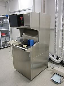
Specific Process Knowledge/Characterization/KLA-Tencor Surfscan 6420
The content on this page, including all images and pictures, was created by DTU Nanolab staff, unless otherwise stated.
Feedback to this page: click here
The KLA-Tencor Surfscan 6420 has has been decommisioned in April 2023 and replaced with the Particle Scanner Takano.
KLA-Tencor Surfscan 6420

The KLA-Tencor is a surface analysis instrument for detecting, couting and sizing of particles, i.e. light point defects. A broad range of particles size from 0.15 µm to greater than 3 µm can be measured on a polished silicon surface with or without or epitaxial layers. The particle contamination in thin films like nitride, oxide and polymer or resist layers can also be inspected. The system will remove small surface roughness, so it will not count as particle contaminations.
The system is mainly being used for quality control of the PECVDs and LPCVD nitride furnaces in the cleanroom.
Users will have to contact the responsible persons (the Thin Film group), if they want to make some particle measurements.
Acceptance Test
We have two calibration wafers for the KLA-Tencor Surfscan. The calibration wafers are 6" silicon wafers with a number of polystyrene latex spheres (PLS) uniformily spread over the surface. Those wafers have been used for the acceptance test. The mean diameter and number PLS's on each wafer are certified.
Calibration wafer 1:
- PLS mean diameter: 0.204 µm +/- 0.008 µm
- Number of PLS's: 7234 +/- 10%
Calibration wafer 2:
- PLS mean diameter: 1.112 µm +/- 0.018 µm
- Number of PLS's: 7700 +/- 10%
Calibration wafer 3:
- PLS mean diameter: 4.000 µm +/- 0.043 µm
- Number of PLS's: 7587 +/- 10%
Repeatability check
Acceptance criterion: 10 scans are done on each of the three PLS calibration wafers. The wafers are loaded/unloaded to the cassette every time. The repeatbility of +/- 1σ has to be less than 1%.
Results:
Calibration wafer 1:
- Measured average PLS diameter: 0.2063 µm. Repeatability: 0,24%
- Average number of PLS's: 7065. Repeatability: 0.11%
Calibration wafer 2:
- Measured average PLS diameter: 1.100 µm. Repeatability: 0%
- Average number of PLS's: 7427. Repeatability: 0.20%
Calibration wafer 3:
- Measured average PLS diameter: 3.970 µm. Repeatability: 0,24%
- Average number of PLS's: 7101. Repeatability: 0.10%
Uniformity check
Acceptance criterion:Measure the average PLS diameter by boxing an area in five different locations on a PLS wafer. The measurement has to be within 3%.
Results:
Calibration wafer 2:
- Non-uniformity: 1,36%
Calibration wafer 3:
- Non-uniformity: 0.38%
Handling test
Acceptance criterion: Run a cassette of 25 wafers. The machine should be able to error-free handle the cassette 40 times, i.e. it should be able to handle 1000 wafers without failing.
Results:
6" cassette": A cassette of 25 wafers was handled 40 times over night, i.e. the acceptance criterion was meet.
4" and 8" cassette: A cassette of 25 wafers was handled two times. The scanning was then stopped to save time as handling of more cassettes is not expected to cause problems.
Process Parameters
| Purpose |
| |
|---|---|---|
| Performance | Particles size |
|
| Througput |
| |
| Repeatbility |
| |
| Process parameter range | Process Temperature |
|
| Substrates | Batch size |
|
| Substrate materials allowed |
|
