Specific Process Knowledge/Characterization/III-V ECV-profiler
Feedback to this page: click here
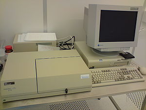
III-V ECV-profiler


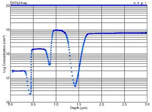
The ECV (Electrochemical Capacitance-Voltage) technique is used to measure carrier-density as a function of depth (doping-profile) on planar semiconductor structures - usually III-V compound semiconductors.
The ECV-profiler is maintained by DTU fotonik (not DTU Nanolab) and is therefor not in LabManager!
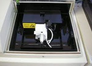
ECV is a destructive technique requiring a sample size of at least 5x5mm and good skills to obtain reproduceable and reliable results. The sample is placed in a electrochemical cell and electrical contacted to form a capacitor. This is done on one side through the electrolyte and on the other side via a ohmic contact on either the front- or the backside (preferred) of the wafer.
Note! We can only offer very limited help for this system. The ECV-profiler is not used very much and it is an old system. It has not been serviced for many years and it is very difficult (impossible) to get spare parts and technical support for it. /jehan
| Performance | Excitation |
|
|---|---|---|
| Detection |
| |
| Sample size |
| |
| Resolution |
| |
| Carrier density accuracy |
| |
| Materials | Allowed substrate materials |
|
