Specific Process Knowledge/Back-end processing/Wire Bonder/TPT HB 100 wire bonder: process details
Feedback to this page: click here
The TPT HB100 Wire Bonder is a versatile semi-automatic system designed for research, prototyping, and small-scale production in microelectronics packaging. It supports multiple bonding methods including wedge–wedge, ball–wedge, and bump bonding. While a single bond head can accommodate all modes, each bonding method requires its own dedicated needles/capillary, or ribbon clamp, which must be mounted before use.
The system is supplied with wires and standard accessories, and at the moment the tool can be configured for either 25 µm diameter gold wire or 33 µm diameter aluminum wire. For changing the wires or needle, users should contact the responsible tool owner.click here
The system is equipped with motorized X, Y, Z axes and bond head rotation, the HB100 ensures precise and flexible operation. The integrated TPT software provides a library of recipe templates, allowing users to quickly create and customize process recipes according to bonding method and wire type.
Note: Height variations greater than 100 µm can lead to bonding failures due to incorrect force and ultrasonic coupling.
Important understanding: The height uniformity across the chip and the PCB has a significant impact on wire bonding performance. When the local surface height varies by more than ~100 µm, the bonder’s programmed bond force and ultrasonic energy may no longer be applied correctly at each pad. Because the tool approaches every bond location using a reference Z-height, a sudden height difference results in either:
Insufficient bond force or ultrasonic coupling (if the pad is lower than expected), leading to weak or missing bonds, or
Excessive tool impact (if the pad is higher than expected), increasing the risk of pad damage or tool wear.
This issue becomes even more pronounced when the chip is glued onto a PCB, as adhesive thickness variations can easily introduce local warpage or tilt. For reliable bonding, all bonding pads on the chip must lie in the same plane, and similarly, the PCB bonding pads should not exhibit large step differences greater than 100 µm can compromise bond quality.
Maintaining flatness of the chip compared to the PCB/substrate are therefore critical to achieve consistent, high-quality wire bonds across the entire device.
Key specifications are summarized below:
| Bonding Specifications | Bonding Methods | Wedge–Wedge, Ball–Wedge & Ribbon bonding |
|---|---|---|
| Bond Head Capability | One head for Wedge & Ball bonding (needle change only) | |
| Speed | 1 wire in ~3 sec | |
| Wire Change Time | ~10 min | |
| Bond Method Change Time | ~5 min | |
| Wire & Ribbon Handling | Gold Wire Diameter | 12–75 µm (0.5–3 mil) |
| Aluminium Wire Diameter | 17–75 µm (0.7–3 mil) | |
| Ribbon Size | Max. 25 × 250 µm (1 × 10 mil) | |
| Ultrasonic & Bonding Parameters | Ultrasonic Frequency | 63.3 kHz Transducer PLL control (110 kHz option) |
| Ultrasonic Power | 0–10 W | |
| Bond Time | 0–5 sec | |
| Bond Force | 10–200 cN | |
| Bonding Tool Size | Ø 1.58 mm × 19 mm (0.0624″ × 0.750″) | |
| Wire Termination | Bond Head Tear or Clamp Tear | |
| Mechanics & Motion Control | Z-Drive / Resolution | Lead screw motor / 0.5 µm |
| Motorized Z Travel | 100 mm (3.9″) | |
| X–Y Drive / Resolution | Linear motors / 0.1 µm | |
| Motorized X–Y Travel | 100 mm (3.9″) | |
| Max. Component Width | 400 mm (15.7″) | |
| Rotation Drive Accuracy | ±0.5° | |
| Control & Interface | Axis Control | Joystick |
| Screen Size | 21″ touchscreen | |
| Software Environment | Industrial PC with Windows | |
| Safety Features | C+ Crash Prevention, Data Backup, Password Protection | |
| Camera & Optics | Camera System | Dual camera (detail & overview) |
| Magnification | Up to 150× | |
| View Mode | Simultaneous detail & overview | |
| Heater Stage | Size | 90 mm Ø surface (mechanical & vacuum clamping; other sizes available) |
| Temperature Range | Up to 200 °C ±1 °C | |
| Temperature Controller | Integrated digital controller | |
| Clamping | Mechanical & vacuum | |
| General | Electrical Requirements | 100–240 V ±10%, 50/60 Hz, max. 10 A |
| Dimensions (W × D × H) | 620 × 750 × 680 mm (24.4″ × 29.5″ × 26.7″) | |
| Weight | 72 kg net |
For detailed information on compatible wires and bonding tools for the HB100, visit the TPT Wires & Tools page.
HB100 Bonding Parameters – 25 µm Gold Wire
The bonding parameters can vary depending on the substrate type, the contact pad materials, chip height, and metal thickness. The ranges listed in the table below were tested using gold wire on both aluminum and gold contact pads. These values can serve as a reference, but process parameters may need to be optimized to ensure reliable bonding performance for different material combinations and device geometries.
| First Bond | Ultrasonic Power (US) | 160 - 200 |
|---|---|---|
| Bond Time | 80-200 | |
| Bond Force | 250-300 | |
| Second Bond | Ultrasonic Power (US) | 200-250 |
| Bond Time | 80-200 | |
| Bond Force | 200-300 | |
| Wire | Wire Diameter | 25 µm (Gold) |
| Wire Detect | First Bond: 20 / Second Bond: 0 | |
| Loop | Loop Height | 500-2500 |
| Tail Mode (Clamp Feed Length) | 500 | |
| Temperature | ||
| Stage (°C) | 50-120 | |
| Bond Positions | First Bond (X1, Y1) | Teach first bond |
| Second Bond (X2, Y2) | Teach second bond |
Bond test with Bond plan
  |
Figures: Bond program setup and execution on the TPT HB100 wire bonder: After defining the package and chip dimensions, a bond plan was created with varying wire lengths, loop heights, and bond directions. The top image shows the number of bond plans made (look under wire) and the bond parameters used, while the bottom image illustrates the completed gold wire connections between chip pads, demonstrating successful automated wire bonding using the defined recipe.
HB100 Bump Parameters – 25 µm Gold Wire
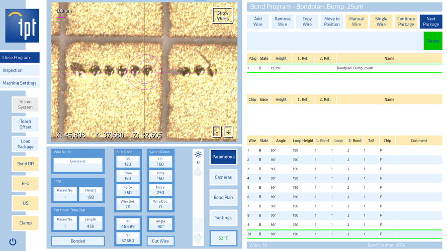
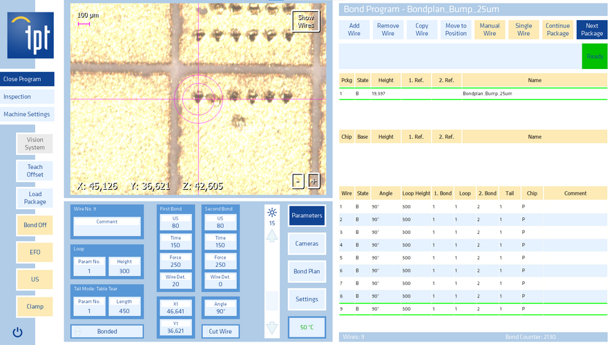
This bond program is designed to form gold bump (stud) structures using 25 µm Au wire on metallized pads. The process employs a Ball-on-Pad (BOP) bonding sequence, in which a free-air ball (FAB) is first formed at the capillary tip by a negative electronic flame-off (EFO) discharge that melts the wire tail into a spherical shape. The tail length is fixed at 450 µm to maintain a consistent ball diameter of approximately three times the wire diameter, ensuring stable and repeatable bump formation. Once the FAB is generated, it is bonded directly onto the pad surface using ultrasonic energy (80 %), a bond force of 250 mN, and a bond time of 150 ms at a stage temperature of 50 °C, with wire detection enabled at 20 % to confirm pad contact. This step creates a solid Au–Au metallurgical interface with controlled deformation. Following the initial bond, the wire is automatically torn off in a second-bond stage using identical ultrasonic and force settings, with wire detection disabled and a loop height of 300 µm to provide clearance for proper wire breakage. The resulting structure is a gold stud bump with a measured foot of 125-140 µm, and 10x repeat for foot and stud height analysis serving as a reliable baseline for further optimization and flip-chip bonding development.
| First Bond | Ultrasonic Power (US) | 80 - 150 |
|---|---|---|
| Bond Time | 50-150 | |
| Bond Force | 200-300 | |
| Second Bond | Ultrasonic Power (US) | 80 |
| Bond Time | 50-150 | |
| Bond Force | 200-300 | |
| Wire | Wire Diameter | 25 µm (Gold) |
| Wire Detect | First Bond: 20 / Second Bond: 0 | |
| Loop | Loop Height | 200 |
| Tail Mode (table tear) | 450 | |
| Temperature | ||
| Stage (°C) | 25 | |
| Bond Positions | First Bond (X1, Y1) | Teach first bond |
| Second Bond (Angle) | 90° |
Bond program


Loop program parameters must be adjusted according to bond length because variations in loop height and span directly influence wire deformation, mechanical stress distribution, and loop stability; optimizing these parameters ensures proper wire trajectory, prevents sagging or breakage, and maintains the electrical and mechanical reliability of the bond.
Bond inspection

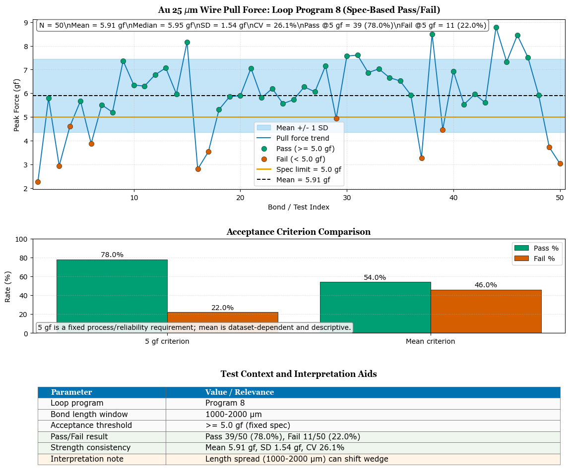
The pull test evaluation of 25 µm Au wire bonds formed using Loop Program 8 demonstrates a mean peak pull force of 5.91 gf with a standard deviation of 1.54 gf across 50 samples. The measured distribution spans from approximately 2.3 gf to 8.8 gf, indicating a relatively broad mechanical response. Using a fixed lower specification limit of 5.0 gf, 78% of the bonds met the acceptance criterion, while 22% failed. The coefficient of variation (26.1%) reflects moderate-to-high process variability, which is expected in a research bonding environment where substrate type, pad metallization, and thermal characteristics differ between devices.
The majority of pull values cluster between 5.5 and 7.5 gf, suggesting that under typical conditions the bond interface achieves adequate metallurgical strength. However, the presence of low-force outliers below 4 gf indicates occasional interfacial weakness, potentially related to surface condition, ultrasonic coupling efficiency, or local geometry variations within the 1000–2000 µm bond length window. Higher-force measurements above 7 gf imply that failure likely occurred in the wire or neck region, which is mechanically desirable.
Au Bump program
 |
 |
Au Bump Formation and Coining
HB100 Bonding Parameters – 33 µm Aluminum Wire
INFO COMING SOON
Comments & Technical Discussion
This section allows users to submit technical feedback, corrections, or improvement suggestions regarding this page.
Please keep comments concise, professional, and data-driven.
All comments will be recorded on the associated discussion page: Talk:Specific Process Knowledge/Back-end processing/Wire Bonder/TPT HB 100 wire bonder: process details
For urgent tool-related matters, please contact:
thcl@dtu.dk or prakus@dtu.dk


