LabAdviser/Technology Research/Fabrication of Hyperbolic Metamaterials using Atomic Layer Deposition/TIO ALU Gratings Procces flow
Feedback to this page: click here
This page is written by Evgeniy Shkondin @DTU Nanolab if nothing else is stated.
All images and photos on this page belongs to DTU Nanolab and DTU Electro (previous DTU Fotonik).
The fabrication and characterization described below were conducted in 2013-2016 by Evgeniy Shkondin, DTU Nanolab.
Procces flow description
All samples were prepared and characterized in a class 100 cleanroom. Si (100) wafers of 150 mm were used as a substrate. The main steps in the gratings manufacturing are shown in a figure below. First, the silicon trenches were realized by deep reactive ion etching (DRIE). Then, the trenches were ALD coated. After the selective removal of the top parts, the silicon core between ALD coatings was etched away during the last step. The final structure represents the highly anisotropic vertical grating. Each fabrication step was carefully inspected using cross-sectional scanning electron microscopy (SEM) imaging.
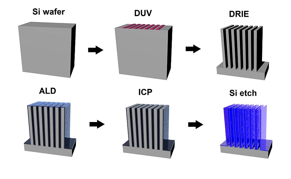
Scheme of fabrication flow. High aspect ratio Al2O3 and TiO2 nanogratings.

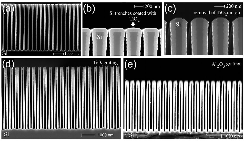
High aspect ratio Al2O3 and TiO2 nanogratings. SEM cross-sectional inspection.

Process flow
Description of steps for fabrication of TiO2 and AL2O3 nanogratings.
| Step | Description | LabAdviser link | Image showing the step | |
|---|---|---|---|---|
| 1.1 | Plasma surface treatment | To ensure clean surface, the 100 mm Si wafer is treated by O2/N2 plasma. (Optional step) | Plasma Asher 2 | _nanogratings.JPG) |
| 1.2 | DUV Resist patterning | DUV | DUV Stepper Lithography. | _nanogratings.JPG) |
| 1.3 | Deep reactive ion etching (DRIE) | DRIE; Recipe: PolySOI10 | DRIE Pegasus. | _nanogratings.JPG) |
| 1.4 | Plasma surface treatment | To ensure that remainings of DUV resist are gone, samples are treated by O2/N2 plasma. (Optional step) | Plasma Asher 2. | |
| 1.5 | Scanning Electron Microscopy inspection | By cleaving the sample it is possible to inspect DRIE etched Si trenches in cross-sectional mode |  | |
| 1.6 | Atomic Layer Deposition of either Al2O3 or TiO2 | Deposition carried at 150C.Thickness is 90 nm. | Equipment used: ALD Picosun R200. Standard recipes used: Al2O3T and TiO2T . | _nanogratings.JPG) |
| 1.7 | Scanning Electron Microscopy inspection | By cleaving the sample it is possible to inspect ALD coatings deposited on Si trenches in cross-sectional mode |  | |
| 1.8 | Opening of deposited Al2O3 or TiO2 top layers. | Etching happens using ICP Metal etcher with Cl2/BCl3 process gasses. | Equipment used: Metal ICP Etcher. | _nanogratings.JPG) |
| 1.9 | Scanning Electron Microscopy inspection | By cleaving the sample it is possible to inspect ICP etcher results Si trenches in cross-sectional mode |  | |
| 1.10 | Selective etch of Si between ALD Al2O3 or TiO2 coatings. | Si etching proceeds using ICP Metal etcher with isotropic process based on SFf process gas. | Equipment used: Metal ICP Etcher. | _nanogratings.JPG) |
| 1.11 | Scanning Electron Microscopy inspection of fabricated structure. | Proof of final result. |  | |
| 1.12 | Ion beam etching. (Optional) | Additional shape of the top part. 20 mijn etch using recipe "Ti acceptance" there the stage shoud be placed to 0o degree. SEM cross section is used for inspection | IBE/IBSD Ionfab 300 |  |