File:WF 2E02 mar23 2011-060.jpg
Size of this preview: 800 × 600 pixels. Other resolution: 1,024 × 768 pixels.
Original file (1,024 × 768 pixels, file size: 114 KB, MIME type: image/jpeg)
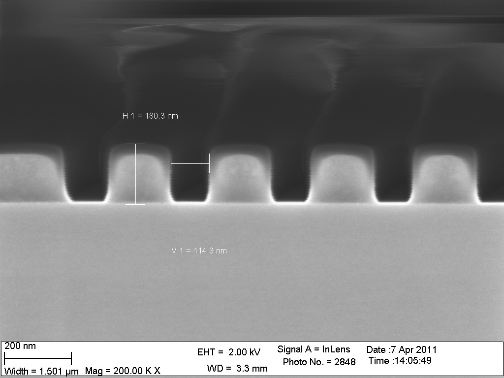
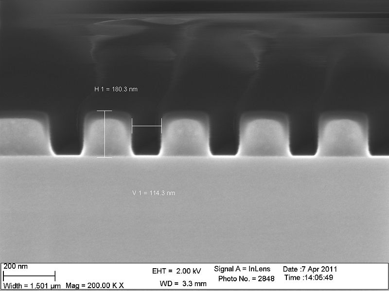
The profiles of the 211 nm thick zep resist wafers (The E-batch of march 23 2011). The wafers have been over-exposed in the E-beam (400 µC/cm2) to make sure that all structures are opened - therefore the 30, 60, 90, 120 and 150 nm lines are somewhat wider.
File history
Click on a date/time to view the file as it appeared at that time.
| Date/Time | Thumbnail | Dimensions | User | Comment | |
|---|---|---|---|---|---|
| current | 15:17, 7 April 2011 | | 1,024 × 768 (114 KB) | Jml (talk | contribs) | The profiles of the 211 nm thick zep resist wafers (The E-batch of march 23 2011). The wafers have been over-exposed in the E-beam (400 µC/cm2) to make sure that all structures are opened - therefore the 30, 60, 90, 120 and 150 nm lines are somewhat wide |
You cannot overwrite this file.
File usage
The following page uses this file: