Specific Process Knowledge/Etch/Etching of Gold
Appearance
Ething of Gold can be done either wet or dry. For wet etching please see below on this page. Dry etching can be done with IBE by sputtering with Ar ions.
Etching of Gold

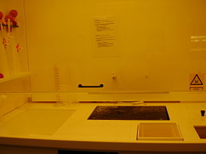
Etching of Gold is done wet at Danchip making your own set up in a beaker in the fumehood. We have two different solutions:
- Iodine etch: KI:I2:H2O - 100g:25g:500ml - standard at Danchip. Can be used with AZ resist as mask.
- Aqua Regia (Kongevand): HNO3:HCl - 1:3 - A very strong acid witch will etch most metals and are therefore used when you wish to remove all the gold from your wafer. you have to be very carefull when you work with Aqua Regia (Kongevand) It can generate nitrous gases witch are very toxic!!
Comparing the two solutions
| Iodine based gold etch | Aqua Regia (Kongevand) | |
|---|---|---|
| General description |
Etch of pure Gold with or without photoresist mask. |
Etch of pure Gold (as stripper). |
| Chemical solution | KI:I2:H2O (100g:25g:500ml) | HCl:HNO3 (3:1) |
| Process temperature | 20 oC | 20 oC |
| Possible masking materials |
Photoresist (1.5 µm AZ5214E) |
Unmasked - used as a stripper |
| Etch rate |
~100 nm/min |
~(??) nm/min - fast etch |
| Batch size |
1-5 4" wafers at a time |
1-5 4" wafer at a time |
| Size of substrate |
2-6" wafers |
2-6" wafers |
Feedback to this page: click here
THIS PAGE IS UNDER CONSTRUCTION
Etching of Gold
Etching of Gold can be done either by wet etch, dry etch or by sputtering with ions.
Comparison of Aluminium Etch Metodes
| Al wet etch 1 | Al wet etch 2 | ICP metal | IBE (Ionfab300+) | |
|---|---|---|---|---|
| Generel description | Wet etch of pure Al | Wet etch of Al + 1.5% Si | Dry plasma etch of Al | Sputtering of Al - pure physical etch |
| Etch rate range |
|
|
|
|
| Etch profile |
|
|
|
|
| Substrate size |
|
|
|
Smaller pieces glued to carrier wafer
|
| Allowed materials |
|
|
|
|
