Specific Process Knowledge/Etch/IBE⁄IBSD Ionfab 300/IBE Ti etch

From LabAdviser
Revision as of 09:35, 22 July 2011 by BGE (talk | contribs) (New page: ==Results from the acceptance test in February 2011== '''Acceptance test for Ti etch:''' {| border="2" cellspacing="0" cellpadding="2" |- !style="background:silver; color:black;" align="l...)
(diff) ← Older revision | Latest revision (diff) | Newer revision → (diff)

Results from the acceptance test in February 2011

Acceptance test for Ti etch:

. Acceptance Criteria

Acceptance Results

Substrate information
  • 50 mm SSP Si wafer
  • 525 µm thick
  • Supplied by Danchip
.
Material to be etched
  • E-beam deposited Ti
.
Mask information
  • E-beam resist mask:
  1. 400nm of spin coated ZEP520A e-beam resist
  2. Patterned by E-beam lithography
.
Features to be etched
  • 300nm - 3µm dots and lines + a square of 200µmx200µm
.
Etch depth
  • 300nm
  • ~270 nm
Etch rate
  • >80nm/min
  • 22nm/min +- 0.3nm/min (one standard deviation)
Etch rate uniformity
  • <+-2%
  • +-(0.2% +-0.2%)
Reproducibility
  • <+-2%
  • +-(0.8% +-0.5%)
Selectivity (Au etch rate/ZEP etch rate)
  • At least 1:1
  • 0.7:1
Etch profile
  • 70-90dg.
  • ~65dg @270nm
  • ~77dg @123nm


Some SEM profile images of the etched Au

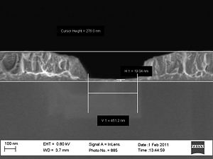
Ti s10-4: 270nm deep - 500nm line. all zep has gone. Profile: ~65 dg.
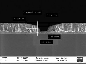
Ti s10-5: 270nm deep - 300nm line. All zep has gone. Profile: ~65 dg.
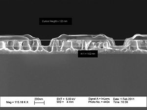
Ti S7 5: 123nm deep - 300nm line. Still zep left. Profile: ~77 dg