Specific Process Knowledge/Lithography/EBeamLithography/JEOLAlignment
Aligned exposure on JEOL 9500
There is quite a few things to remember in order to align an exposure to an existing pattern. The example below is a step by step guide illustrating global substrate alignment as well as chip alignment. If your job only requires global alignment simply skip the chip alignment part. In the example we assume a layer, L1, is already defined on the substrate and the goal is to align the next layer, L2, to it.
The job is also explained in a tutorial video found here.
Job preparation
The job illustrated below writes a chip layout in a 5 x 5 matrix into a 2 x 2 matrix as illustrated in the figure. The first layer, L1, has defined global marks at P = (-30000,0) and Q = (30000,0). The local chip marks are placed at M1 = (-450,450), M2 = (450,450), M3 = (450,-450) and M4=(-450,-450). First a global alignment is called via the GLMDET command and subsequently chip alignment is called using the CHIPAL command. The mark positions are stated in the JDF file using the GLMPOS command for PQ marks and the M1 to M4 commands for chip marks. Remember that a V30 file is placed relative to its bounding box center coordinate and hence it might be necessary to control the bounding box extents by adding control geometry (corner marks) if the design is not symmetric around (0,0) in the chip design coordinate system.
The following SDF and JDF files will be used for the example.
;SDF
MAGAZIN	'THOPE'

#7
%4D
JDF	'thope230126',1
ACC 100
CALPRM '6na_ap5'
DEFMODE 2
GLMDET A
CHIPAL 1
HSWITCH OFF,ON
RESIST 250
SHOT A,24
OFFSET(88,-335)

END 7
;JDF
JOB/W    'THOPE',4  ; 4inch wafer

GLMPOS    P=(-30000,-20000),Q=(30000,20000)

PATH FT01
  ARRAY	(-15000,2,30000)/(10000,2,20000)
	ASSIGN A(1) -> ((*,*))

1: 	ARRAY (-4000,5,2000)/(4000,5,2000)
	CHMPOS M1=(-450,450),M2=(450,450),M3=(450,-450),M4=(-450,-450)
	ASSIGN P(1) -> (*,*)

  AEND
PEND

LAYER	1
        P(1)  'thope230126.v30'
        SPPRM 4.0,,,,1.0,1
        STDCUR  6.6
        OBJAPT 5

END
Optical pre-alignment
The optical pre-aligner is used to measure the location of the P and Q marks of the substrate after loading it to a cassette. The optical pre-alignment procedure will output several useful numbers:
- P mark stage coordinate
- Q mark stage coordinate
- P mark shift relative to the slot center
- Substrate rotation
- Gain
To get started using the prealigner, place the cassette front side down and the hook away from yourself. Log in on the computer and load PAMS Metrology Tool and PAMS Image Viewer. Verify that the coordinate output is correct by moving to the stage zero marker mounted on the bottom right of the prealigner, zero it on the coordinate display panel if it is more than a few µm off.
Move the stage to the center of your substrate, use the coordinates posted on the wall to find it easily. Find a feature that allows you to gauge the rotation, this can be a long straight line or two features that have the same Y-coordinate. Minimize the rotation by either rotating the slot using the set screws (not all cassettes have this) or by removing the substrate cover and rotate the substrate inside the slot. Rotation should be so low that the Y-coordinate difference between the P and Q marks is less than 500 µm.
 |

|
|
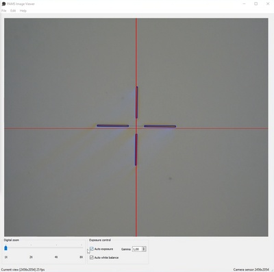
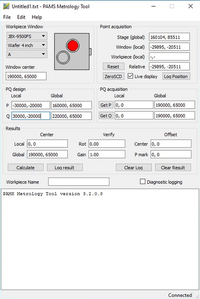
Prealignment using the PAMS Metrology Tool and PAMS Microscope view. Image: Thomas Pedersen. | |
It is usually a good idea to deal with substrate rotation first. Move the stage to the center of your substrate. Use the coordinate guide posted on the wall next to the prealigner and the coordinate read out on the table. Once you find the center of your substrate move to a horisontal feature like a cross or waveguide that will allow rotation adjustment. In the example below we have a cross (the P mark) which is obviously rotated relative to the red cross hair.
If the cassette has a slot rotation screw, use this to roughly correct rotation. If the slot does not have a rotation screw, remove the substrate cover and rotate your substrate. The rotation screw is fragile, NEVER USE A TOOL TO ROTATE IT. Only use your fingers. The slot is spring loaded, if it is hard to turn the screw you can release tension in the springs by firmly presseing down on the outer ring as illustrated below.
Once the substrate rotation is fine it is time to find the actual alignment marks (P and Q marks). In the Metrology tool choose “JBX-9500FS” on the “Workpiece Window” dropdown and choose the substrate size and slot ID of your substrate. Enter the design coordinates of the P and Q marks in the “PQ design Local” fields.
Now find your P mark, align it to the red cross hair at 8X digital zoom and click “Get P”. Click it a few times as the first time always inputs an incorrect coordinate. Move to your Q mark, align to the cross hair and click “Get Q” a few times. Now click “Calculate”. The software will now calculate the rotation and gain. Verify that rotation is better than ± 0.5°, if not you should rotate the slot as described above. Substrate rotation and finding the P and Q marks can be an iterative process and you should continue to ensure that rotation is better than ± 0.5°. Also verify that the gain is close to 1. The gain is the ratio of measured distance between P and Q marks versus the design distance, ideally it should be 1. Finally press “Log result” to produce a text output. Copy and paste the output into a text file and save it with your exposure files, for instance to your M-drive. The procedure must naturally be carried out for all substrates that need alignment exposure. When you are done with the alignment station, please close the programs, log off the computer and turn the microscope illumination down. Alert a member of the loading team to have your prealigned substrates loaded to the auto stocker.
PAMS Metrology Tool version 3.2.0.8

JBX-9500FS Wafer 4 inch A <>
Registration result recorded 09-maj-2023, 11:15
 Global mark P: design (-30000,-20000), stage (160108, 85480)
 Global mark Q: design ( 30000,-20000), stage (220107, 85909)
 Material  cc : offset (   250,  -695), stage (190250, 65695)

 Gain	1.00001
 Rotation	0.41 degrees
 OFFSET(   108,  -480) ;(P mark)
end<>
System calibration
Execution of an aligned exposure has the same initial calibration steps as an unaligned exposure, i.e. it has the following steps
- Select and restore the system to the chosen beam current profile (RESTOR)
- Execute a current measurement (CURRNT)
- Execute absorbed electron mark detection (INITAE)
- Execute backscatter electron mark detection (INITBE)
- Execute self calibration routine daily
- Verify drift is low (DRIFT)
- Map height profile of sample (HEIMAP)
After sample height verification follows a few aditional steps to verify the system can find the substrate alignment marks.
Auto Gain Correction - AGCRG
Alignment is done by scanning the beam over the alignment marks and recording the backscatter electron intensity. Thus, it is essential that the gain of the detector system is set to match the substrate material, the mark material and the beam current. The system can automatically optimize the gain of the backscatter detector through the AGCRG subprogram. Bear in mind, it is not always possible to get sufficient signal. Al alignment marks on a Si substrate will for instance basically never work since the atomic number and hence backscatter intensity of the two materials are almost the same.

