Specific Process Knowledge/Etch/ICP Metal Etcher/Chromium/Cr etch data from AS
Feedback to this page: click here
Test data on Cr etch development by Anders Simonsen @NBI.KU 

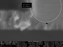
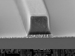
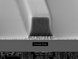
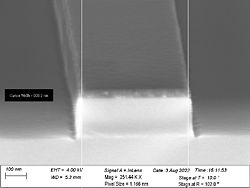
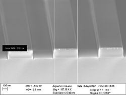
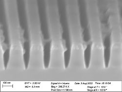
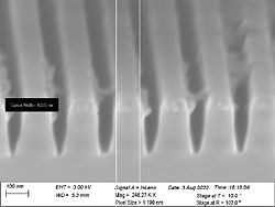
DOE experiments and results made on pattern free samples and samples patterned with UV lithography (SEM images)
| Name | Pressure [mTorr] | Coil power [W] | Platen power [W] | Total Flow (Cl2+O2) [sccm] | O2 % | Selectivity | Etch-rate [nm/min] | Side-angle | Corner | Resist-damage | Etch time [s] | Etch depth [nm] | Angle1 | Radius1 | Angle2 | |
|---|---|---|---|---|---|---|---|---|---|---|---|---|---|---|---|---|
| t5 | 5 | 300 | 25 | 40 | 25 | 0.21 | 49.03 | 25.5 | 319.5 | 1 | 175 | 57 | 28 | 331 | 23 | |
| t7 | 15 | 300 | 15 | 40 | 15 | 0.61 | 52.15 | 12 | 154.5 | 1 | 130 | 87 | 14 | 159 | 10 | |
| t8 | 5 | 500 | 15 | 40 | 25 | 0.4 | 49.50 | 39.5 | 228.5 | 1 | 120 | 101 | 42 | 169 | 37 | |
| t4 | 15 | 500 | 25 | 40 | 15 | 0.39 | 70.80 | 19.5 | 201 | 1 | 100 | 82 | 21 | 158 | 18 | |
| t2 | 5 | 300 | 25 | 80 | 15 | 0.21 | 40.54 | 40.5 | 262.5 | 3 | 185 | 75 | 42 | 274 | 39 | |
| t10 | 15 | 300 | 15 | 80 | 25 | 0.68 | 58.00 | 11.5 | 87 | 2 | 120 | 84 | 14 | 70 | 9 | |
| t6 | 5 | 500 | 15 | 80 | 15 | 0.43 | 49.24 | 29.5 | 300 | 5 | 145 | 81 | 29 | 362 | 30 | |
| t9 | 15 | 500 | 25 | 80 | 25 | 0.41 | 80.67 | 18.5 | 134.5 | 2 | 90 | 79 | 20 | 155 | 17 | |
| t1 | 10 | 400 | 20 | 60 | 20 | 0.35 | 63.13 | 17.5 | 288 | 2 | 115 | 79 | 20 | 292 | 15 | |
| t1R | 10 | 400 | 20 | 60 | 20 | 0.4 | 57.14 | 20 | 186 | 2 | 105 | 100 | 24 | 232 | 16 |
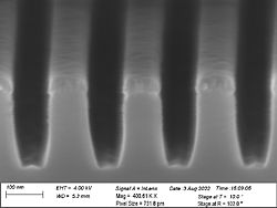
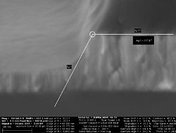
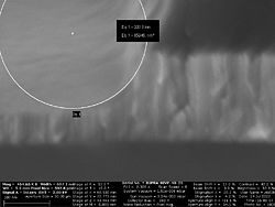
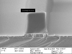
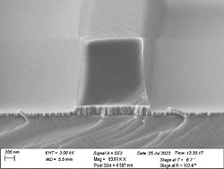
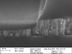
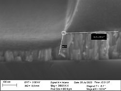
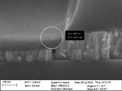
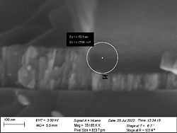
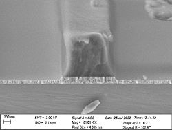
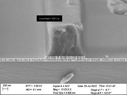
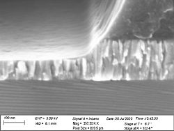
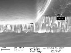
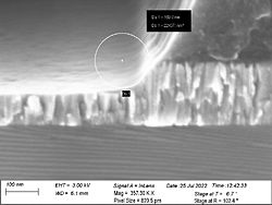
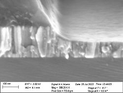
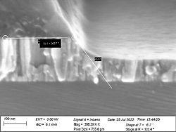
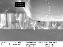
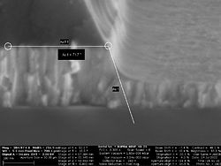
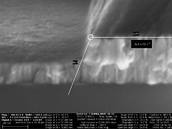
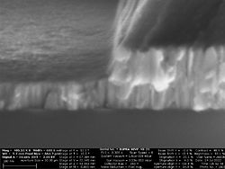
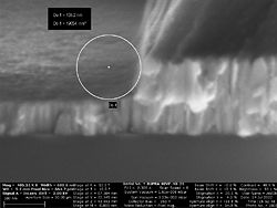
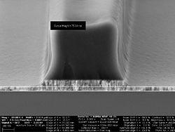
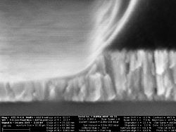
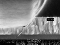
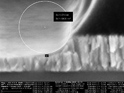
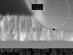
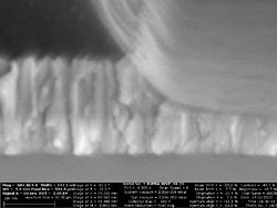
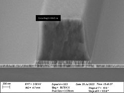
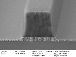
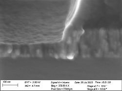
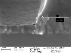
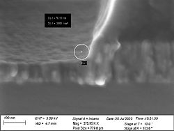
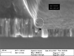
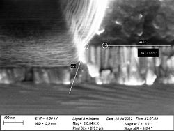
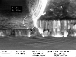
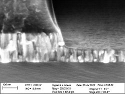
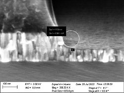
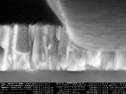
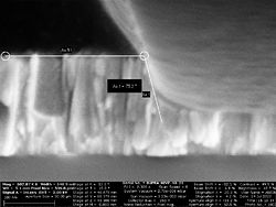
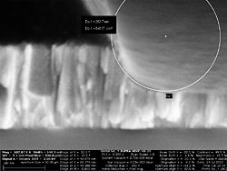
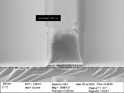
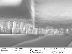
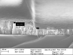
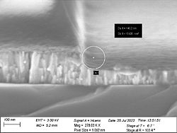
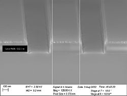
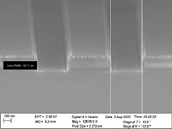
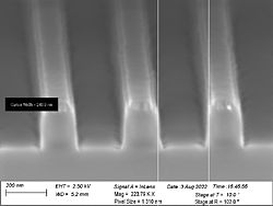
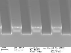
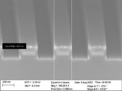
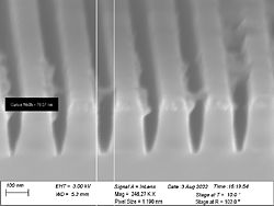
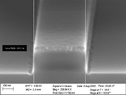
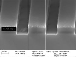
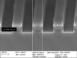
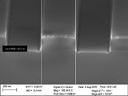
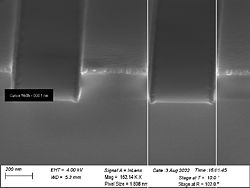
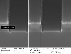
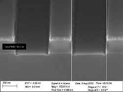
Sem images of the DOE
- Sample t5
-
-
-
-
-
-
-
-


- Sample t7
-
-
-
-
-
-
-
-


- Sample t8
-
-
-
-
-
-
-
-


- Sample t4
-
-
-
-
-
-
-
-


- Sample t2
-
-
-
-
-
-
-
-


- Sample t10
-
-
-
-
-
-
-
-


- Sample t9
-
-
-

-
-
-
-
-


- Sample t1
-
-
-
-
-
-
-


- Sample t1R
-
-
-
-
-
-
-
-


Tests made after DOE with e-beam patterned samples
| Recipe | Pressure [mTorr] | Coil power [W] | Platen power [W] | Total Flow Cl2+O2 [sccm] | O2% | Temp | Time [s] | CSAR etch rate [nm/min] | CSAR rate w bond | Etch rate [nm/min] | Selectivity | coil load | coil tune | plat load | plat tune | Comment | |||
|---|---|---|---|---|---|---|---|---|---|---|---|---|---|---|---|---|---|---|---|
| test11 | 15 | 300 | 15 | 40 | 25.00 | 20 | 23 | 80.87 | 73 | 52.17 | 0.65 | ||||||||
| test12 | 20 | 300 | 15 | 30 | 23.33 | 20 | 21 | 65.71 | 56 | 57.14 | 0.87 | ||||||||
| test13/laqs | 10 | 300 | 15 | 30 | 23.33 | 20 | 28 | 100.71 | 42.86 | 0.43 | Default recipe used for Cr etching when unspecified | ||||||||
| test14 | 10 | 300 | 15 | 40 | 25.00 | 20 | 30 | 88.00 | 40.00 | 0.45 | |||||||||
| nano | 5 | 500 | 15 | 60 | 0.17 | 10 | 33 | 99.00 | 36.36 | 0.37 | 41 | 52 | 31 | 50 | With strike pressure | ||||
| langman | 10 | 500 | 25 | 40 | 0.20 | 8 | 21 | 168.39 | 57.14 | 0.34 | 42 | 52 | 35 | 53 | With strike pressure |
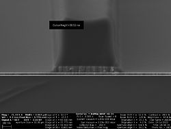
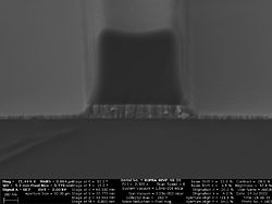
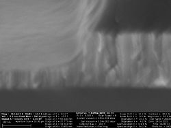
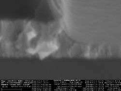
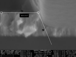
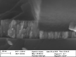
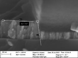
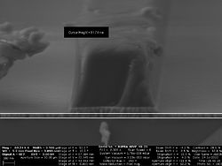
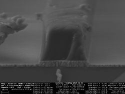
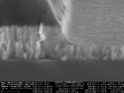
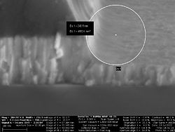
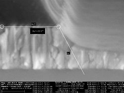
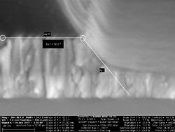
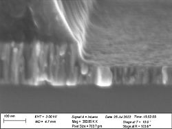
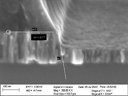
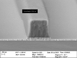
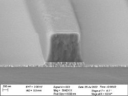
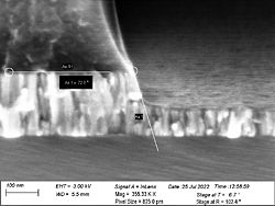
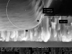
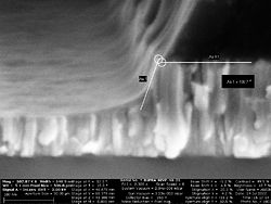
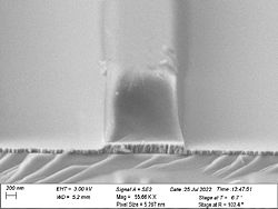
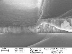
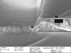
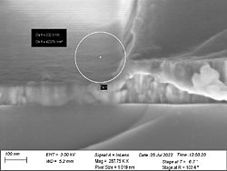
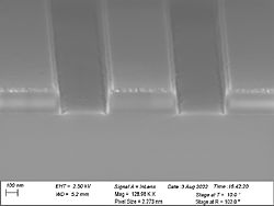
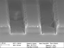
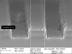
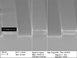
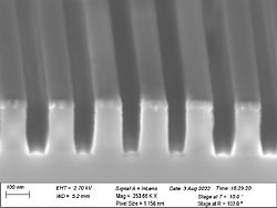
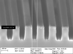
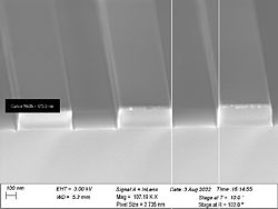
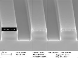
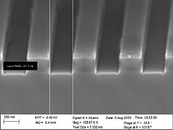
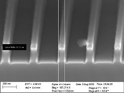
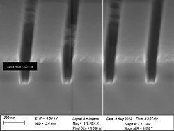
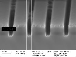
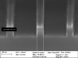
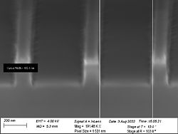
SEM images of the tests after the DOE
These SEM images where done after both the Cr etch and the silicon nitride etch in the ICP metal using the recipe "Slow etch with carrier". The important thing was to see how well the Cr work for masking the nitride given vertical and smooth sidewalls.
- Sample test11
-
-
-
-
-
-

-

-


- Sample test12 2 min
-
-

-
-
-

-
-

-


- Sample test13
-
-
-
-
-

-
-
-


- Sample testnano
-
-
-

-
-
-
-
-


- Sample elangman
-
-
-
-
-
-
-