Specific Process Knowledge/Etch/DRIE-Pegasus/Nanoscale silicon etching with SF6 and O2
Feedback to this page: silicon etching with SF6 and O2 click here
The CORE sequence (meaning Clear, Oxidize, Remove and Etch) is a fluorocarbon-free directional plasma etch procedure that enables a higher selectivity, creates pattern independence of etching profiles and works excellent at room temperature. The CORE process resembles the well-known SF6-based Bosch process, but the usual C4F8 inhibitor is replaced by O2 oxidation with self-limiting characteristics. Therefore the CORE result is similar to Bosch, however has the advantage of preventing the pile-up of fluorocarbon deposits at the topside of deep-etched or nano-sized features. At the same time, process drift is minimized as the reactor wall is staying perfectly clean. The CORE process has shown an excellent performance in high aspect ratio (3D) nanoscale structures with an accurate and controllable etch rate between 1 and 50 nm min−1 (and SiO2-selectivity of ca. 35) using the etch-tool in the RIE-mode. By adding the ICP source (DRIE-mode), a directional etch rate up to 1 μm min−1 (at 50 sccm SF6 flow) and selectivity >200 for SiO2 is possible.
The CORE recipe is shown as below
The CORE cycle design rules and optimized recipe for the etch rate fixed at 15 nm\min
Rule 1: 2 min E-time needs 2 s O-time. Every 2 min extra E-time will need 1 s extra O-time until a maximum of 14 min E-time.
Rule 2: Every second of O-time needs at least 3 s R-time (for 8 min E-time).
Rule 3: The undercut is roughly half of the gained etch depth per CORE cycle.
Silicon wafers are prepared with 1.5 μm thick resist patterns (AZ MIR 701 DUV resist from MicroChemicals) and exposed using a maskless aligner (MLA150, Heidelberg) to create patterns above 400 nm.
For nanosized patterns between 30 and 100 nm, an electron beam writing system (JEOL JBX-9500FSZ) is used with positive tone e-beam resist ZEP520A (ZEON).
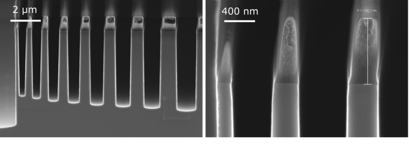
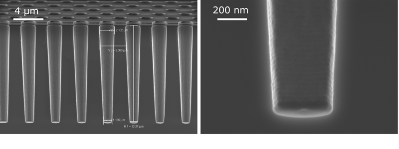
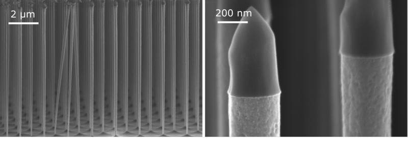
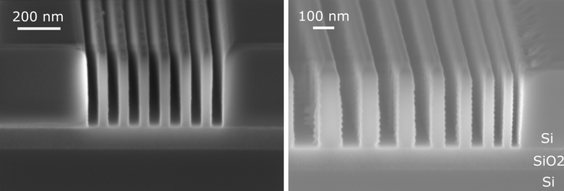
Below are some SEM images of the silicon nanostructures achieved by the CORE process:


For more details, please contact Henri Jansen (henrija@dtu.dk) or Vy Thi Hoang Nguyen (vthongu@dtu.dk).

