Specific Process Knowledge/Characterization/III-V ECV-profiler
Appearance
Feedback to this page: click here
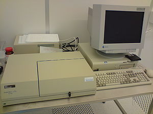
III-V ECV-profiler


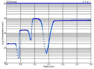
The ECV (Electrochemical Capacitance-Voltage) technique is used to measure carrier-density as a function of depth (doping-profile) on planar semiconductor structures - usually III-V compound semiconductors.
The ECV-profiler is maintained by DTU fotonik (not DTU Nanolab) and is therefor not in LabManager!
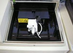
ECV is a destructive technique requiring a sample size of at least 5x5mm and good skills to obtain reproduceable and reliable results. The sample is placed in a electrochemical cell and electrical contacted to form a capacitor. This is done on one side through the electrolyte and on the other side via a ohmic contact on either the front- or the backside (preferred) of the wafer.
| Performance | Excitation |
|
|---|---|---|
| Detection |
| |
| Sample size |
| |
| Resolution |
| |
| Carrier density accuracy |
| |
| Materials | Allowed substrate materials |
|
