Specific Process Knowledge/Thin film deposition/Deposition of Copper/Deposition of Copper
Roughness of Cu layers
The roughness of Cu layers deposited in the Alcatel was examined by AFM measurements.
Experimental
Cr was deposaited in Alcatel, directly on unprocessed Si wafers. The deposition rate was 10 Å/s (the thickness of the layers were between 70 nm and 200 nm).
Results
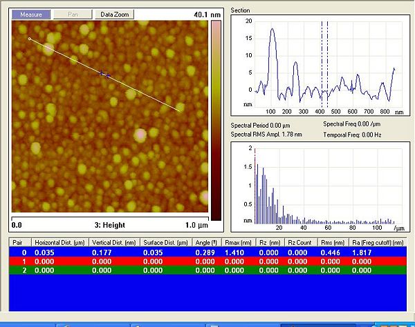
The Cu surface is rather un-uniform. Large grains, randomly distributed, can be seen on the film surface. The largest part of the surface consists of smaller, spherical grains, with a diameter of about 25-40 nm. These are seen in the AFM picture with a height of a few nm, as can be observed below. The largest grains are upp to 70 nm in diameter, and have a height of up to 20 nm.

AFM picture of a Cu surface deposited in Alcatel. A profile of the surface is shown to the right, where the height of some structures can be seen.
