Specific Process Knowledge/Etch/III-V ICP/InP-InGaAsP-InGaAs
Feedback to this page: click here
InP/InGaAsP/InGaAs etch
Unselective etch for large sized features and small aspect ratios by David Larsson, DTU Photonics, 2011
| Recipe | InP Etch 1/InP Precond 1 |
| Cl2 flow | 20 sccm |
| N2 flow | 40 sccm |
| Ar flow | 10 sccm |
| Platen power | 100 W |
| Coil power | 500 W |
| Pressure | 2 mTorr |
| Platen chiller temperature | 180 oC |
| Results (InP Etch 1) | |
| Etch rate | 500-600 nm/min |
| Sidewall angle | 86-87 o |
| Selectivity (InP:SiO2, InP:HSQ) | 50:1 |
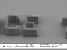
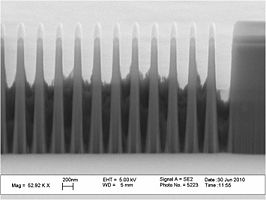
- Result of InP etching. David Larsson, DTU Photonics, 2011
-
-


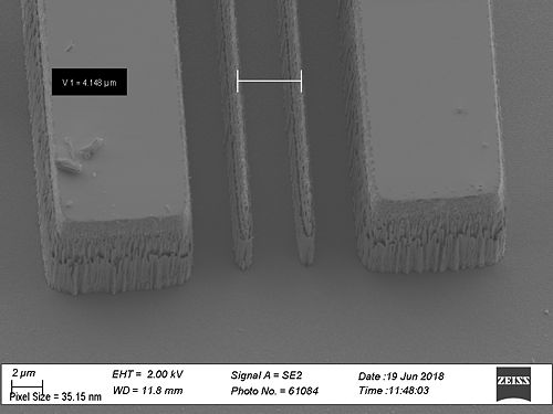
InP etching June 2018
Etching of an InP piece on Si carrier
InP piece patterned with SiO2. The piece was etched on top of a Si wafer without bonding. The recipe "InP etch" was used. The roughness looks high in the bottom of the etched areas, especially the large open areas.
- Result of InP etching.
-
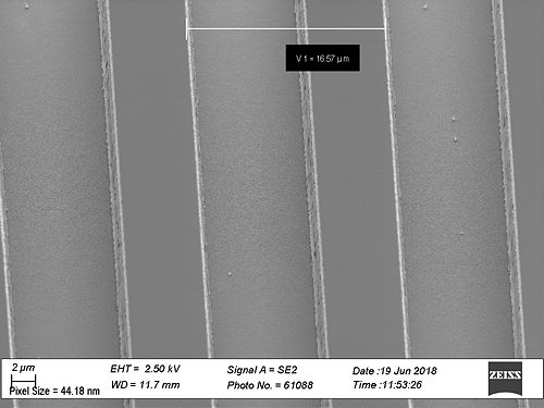
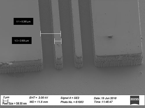 low roughness in narrow trenched
 -
 low roughness in narrow trenched
 -
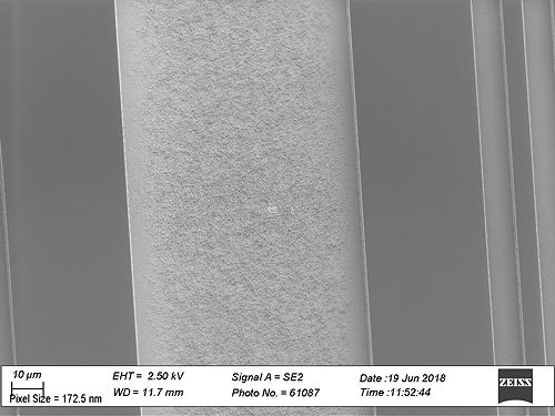
 A little higher roughnedd is larger trences
 -
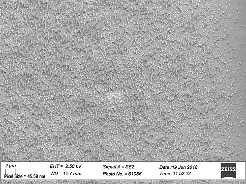
 Much larger roughness in open areas
 -
 Zoom in on the large roughness
 -
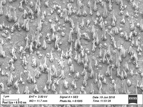 closed look at the large roughness in the open areas.


