Specific Process Knowledge/Etch/Aluminum Oxide/Al2O3 Etch with III-V ICP
Feedback to this page: click here
THIS PAGE IS UNDER CONSTRUCTION
Abstract
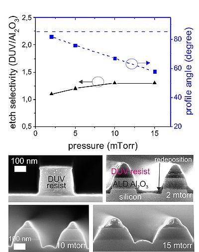
Al2O3 thin-film deposited by atomic layer deposition is an attractive plasma etch mask for MEMS and NEMS. 20-nm-thick Al2O3 mask enables through silicon wafer plasma etching. Al2O3 is also an excellent etch mask for other important MEMS materials such as silicon dioxide, silicon nitride, and diamond. In this report, we systematically study nanoscale plasma etching of Al2O3 with electron beam lithography and deep UV resist masks. The gas composition and pressure were tuned for optimal etching, and redeposition conditions were mapped. With a BCl3 and Ar plasma chemistry, the Al2O3 etch rate was controlled to between 0.1 to 1 nm/min. The etch selectivity of resist over Al2O3 ranged between 4:1 to 1:1. Etch-rate was linearly dependent on the substrate bias power. The etch profile angle can be controlled to between 20 and 82° that almost preserved the resist profile angle. For Al2O3 patterned with deep UV lithography, the smallest structures were 220 nm. For electron beam lithography patterns, the smallest gratings were 18-nm-wide with 50-nm-pitch. Using alumina as a hard mask, we show aspect ratio of 7-10 for subsequent silicon plasma etching. Based on these studies, we provide guidelines for alumina plasma etching on the nanoscale.
For details please contact Anpan Han, e-mail: anph@dtu.dk

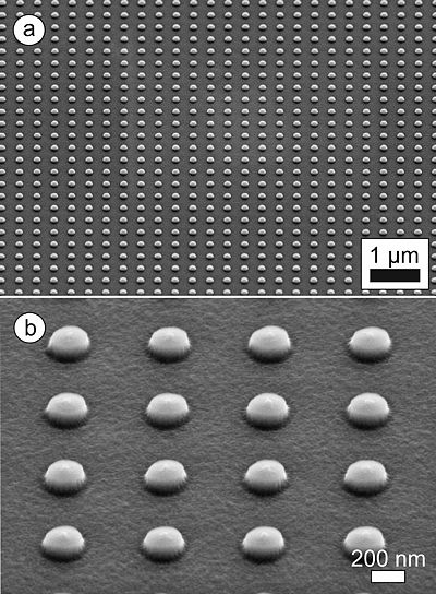
Figure 1. 100-nm-thick ALD Al2O3 films deposited on silicon wafer were patterned using DUV lithography and ICP etched with a BCl3 and Ar plasma.

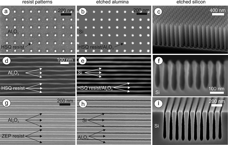
Figure 2. EBL nanopattern transferred into silicon with ALD alumina hard mask and ICP etching. SEM images of EBL HSQ resist nanopatterns of disc arrays (a) on 10-nm-thick ALD alumina coated Si wafer. Resist patterns were etched exposing the underlying silicon (b), and the hard mask was used for pattern transfer to etch silicon pillar arrays. (c) was a tilted image of Si pillar arrays. (d) shows HSQ gratings that were transferred into the alumina film (e), which was used as a hard mask for silicon etch. (f) shows a cross-section image of the etched silicon. ZEP resist gratings (g) transferred into the alumina film (h), and the grating patterns were etched into the silicon (i).

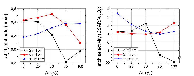
Figure 3. The influence of plasma chemistry and pressure on alumina etch rate and selectivity to the CSAR EBL resist. The plasma contained Ar and BCl3 mixture. All other plasma parameters were kept constant.

Figure 4. ICP pressure effects on the alumina etch profile angle and etch selectivity of DUV resist over alumina. SEM cross-section images of DUV resist gratings before etching, after 2mTorr etch, 10 mTorr etch, and 15 mTorr etch. The remaining DUV resist was not removed before cleaving and SEM imaging. A thin layer of Au was sputter on top of the resist to avoid charging during SEM imaging.
Conclusions and process guidelines
To avoid redeposition, an oxygen plasma chamber conditioning step is required before alumina etching. For etching thicker alumina films, we recommend 2 mTorr, 25% Ar, 75% BCl3. A 5 mTorr and 50% BCl3 plasma is more robust in terms of plasma stability and resist selectivity, but it has an inferior etch profile. Unfortunately, both plasmas will lead to redeposition when etching the underlying silicon layer. For thinner alumina films and breaking through to underlying silicon, we recommend 10 mTorr, 100% BCl3 plasma, but this process will quickly erode the resist mask. If trace amounts of alumina can be tolerated and resist erosion must be kept at a minimum, we recommend a 50% BCl3 plasma at 10 mTorr. We recommend the lowest possible substrate bias for anisotropic etch, and high bias for low profile angle.
| Parameter | Recipe name: no name yet (testing recipe) |
|---|---|
| Coil Power [W] | 1200 |
| Platen Power [W] | 200 |
| Platen temperature [oC] | 0 |
| BCl3 flow [sccm] | 60 |
| Cl2 flow [sccm] | 30 |
| Pressure [mTorr] | 4 |
| Material to be etched | Etch rate using the above parameters |
|---|---|
| Al2O3 |
|
