Specific Process Knowledge/Thin film deposition/MVD
The Molecular Vapor Deposition Tool

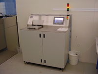
The Applied Microstructures MVD 100 system deposits molecular films on surfaces. These films serve a wide range of purposes ranging from antistiction coatings of nanoimprint lithography stamps to protecting MEMS structures. At Danchip the MVD is essential for nanoimprint lithography.
Processing on the MVD
The MVD coatings are created as self-assembled monolayers on a surface when a molecular vapor of chemials is present.
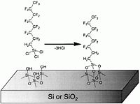
These chemicals, typically it is flourinated organosilanes, have a teflon-like tail consisting of -(CF2)xCF3 and, in the other end, a reactive group -Si(teflon)Clx. As shown in the figure below, the chlorine atoms react with -OH groups of the surface to form a chemical bond -Si((teflon))-O-Si(surface)- under elimination of HCL. This means that both Si and SiO2 surfaces are coated because of the native oxide on Si surfaces.
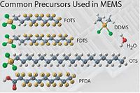
- Some chemicals of the MVD and the surface reaction
-
Different chemicals for the MVD.
-
The chemical reaction in which the Cl atoms of the precursors are eliminated under formation of HCl.
The parameters of the MVD process
The most important parameters to control during the MVD process are:
- Substrate surface
- A O2 plasma is run prior to any process in order to condition the substrate surface. This will also remove any existing MVD coating.
- Water content
- Water will cause the chemicals to polymerize (bond to each other instead of on the surface) and it is therefore critical to precisely control the water content.
- Substrate temperature
- The temperature of the substrate is the same as the process chamber and it is kept constant at 35 oC.
- Vapor order
- There is no active force that injects the chemicals into the process chamber. The driving force is a combination of two factors:
- A pressure gradient The vapor pressure of the chemical (when stored at some temperature in the cylinder) compared to the pressure in the chamber.
- A temperature gradient The chemical and the line that feeds the process chamber are kept at a higher temperature.
It is critical that the chemicals with the lowest vapor pressure are injected first into the process chamber.
The FLAT recipe
The FLAT recipe is designed to coat non-structured wafers.
| O2 plasma | Flow | 200 sccm |
|---|---|---|
| Power | 250 Watts | |
| Time | 300 seconds | |
| Chemical # 1 (vapor order 1) | Name | FDTS |
| Line no. | 3 | |
| Cycles | 4 | |
| Pressure | 0.500 Torr | |
| Chemical # 2 (vapor order 2) | Name | Water |
| Line no. | 1 | |
| Cycles | 1 | |
| Pressure | 18 Torr | |
| Processing | Time | 900 seconds |
| Purge | Cycles | 5 |


